26 www.xilinx.com Virtex-5 FPGA ML561 User Guide
UG199 (v1.2.1) June 15, 2009
Chapter 3: Hardware Description
R
Table 3-6 describes all the signals associated with QDRII component memories.
X
APP853: QDR II SRAM Interface for Virtex-5 Devices and its corresponding demo are
included on the CD shipped with the ML561 Tool Kit.
For a complete list of FPGA #3 signals and their pin locations, refer to Appendix A, “FPGA
Pinouts.”
Table 3-7 describes all signals associated with RLDRAM II devices.
X
APP852, RLDRAM II Memory Interface for Virtex-5 FPGAs and its corresponding demo are
included on the CD shipped with the ML561 Tool Kit.
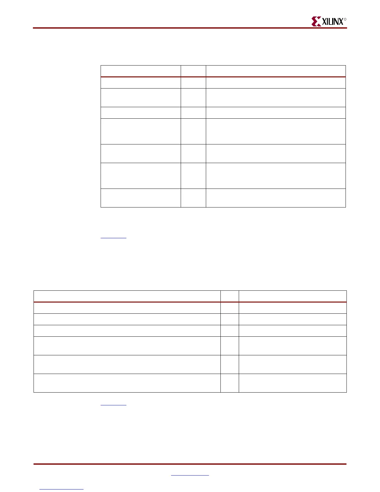
Table 3-6: QDRII Component Signal Summary
Board Signal Name(s) Bits Description
QDR2_SA[18:0] 19 QDRII Address
QDR2_CK_BY0_3_[P,N],
QDR2_CK_BY4_7_[P,N]
4QDRII Differential Clock
QDR2_[R,W,DLL_OFF]_N 3 QDRII Control Signals
QDR2_D_BY[3:0]_B[8:0],
QDR2_K_BY0_3_[P,N],
QDR2_BW_BY[3:0]
42 QDRII Write Data, Strobes, and Byte Write: Bytes 3:0
QDR2_Q_BY[3:0]_B[8:0],
QDR2_CQ_BY0_3_[P,N]
38 QDRII Read Data and Strobes: Bytes 3:0
QDR2_D_BY[7:4]_B[8:0],
QDR2_K_BY4_7_[P,N],
QDR2_BW_BY[3:0]
42 QDRII Write Data, Strobes, and Byte Write: Bytes 7:4
QDR2_Q_BY[7:4]_B[8:0],
QDR2_CQ_BY4_7_[P,N]
38 QDRII Read Data and Strobes: Bytes 7:4
Notes:
1. QDR2_SA[18] is incorrectly labeled QDR2_NC_A3 in the ML561 schematics and layout file.
Table 3-7: RLDRAM II Component Signal Summary
Board Signal Name(s) Bits Description
RLD2_A[19:0], RLD2_BA[2:0] 23 RLDRAM II Address
RLD2_CK_BY0_1 _[P,N] 2 RLDRAM II Differential Clock
RLD2_CK_BY2_3 _[P,N] 2 RLDRAM II Differential Clock
RLD2_CS_BY[0_1,2_3]_N, RLD2_[REF,WE]_N,
RLD2_DM_BY[0_1,2_3]_N, RLD2_QVLD_BY[0_1,2_3]
8 RLDRAM II Control Signals
RLD2_DQ_BY[1:0]_B[8:0], RLD2_DK_BY0_1_[P,N],
RLD2_QK_BY[1:0]_[P,N]
24 RLDRAM II Data and Strobes: Bytes 1:0
RLD2_DQ_BY[3:2]_B[8:0], RLD2_DK_BY0_1_[P,N],
RLD2_QK_BY[3:2]_[P,N]
24 RLDRAM II Data and Strobes: Bytes 3:2
 Loading...


