Virtex-5 FPGA ML561 User Guide www.xilinx.com 131
UG199 (v1.2.1) June 15, 2009
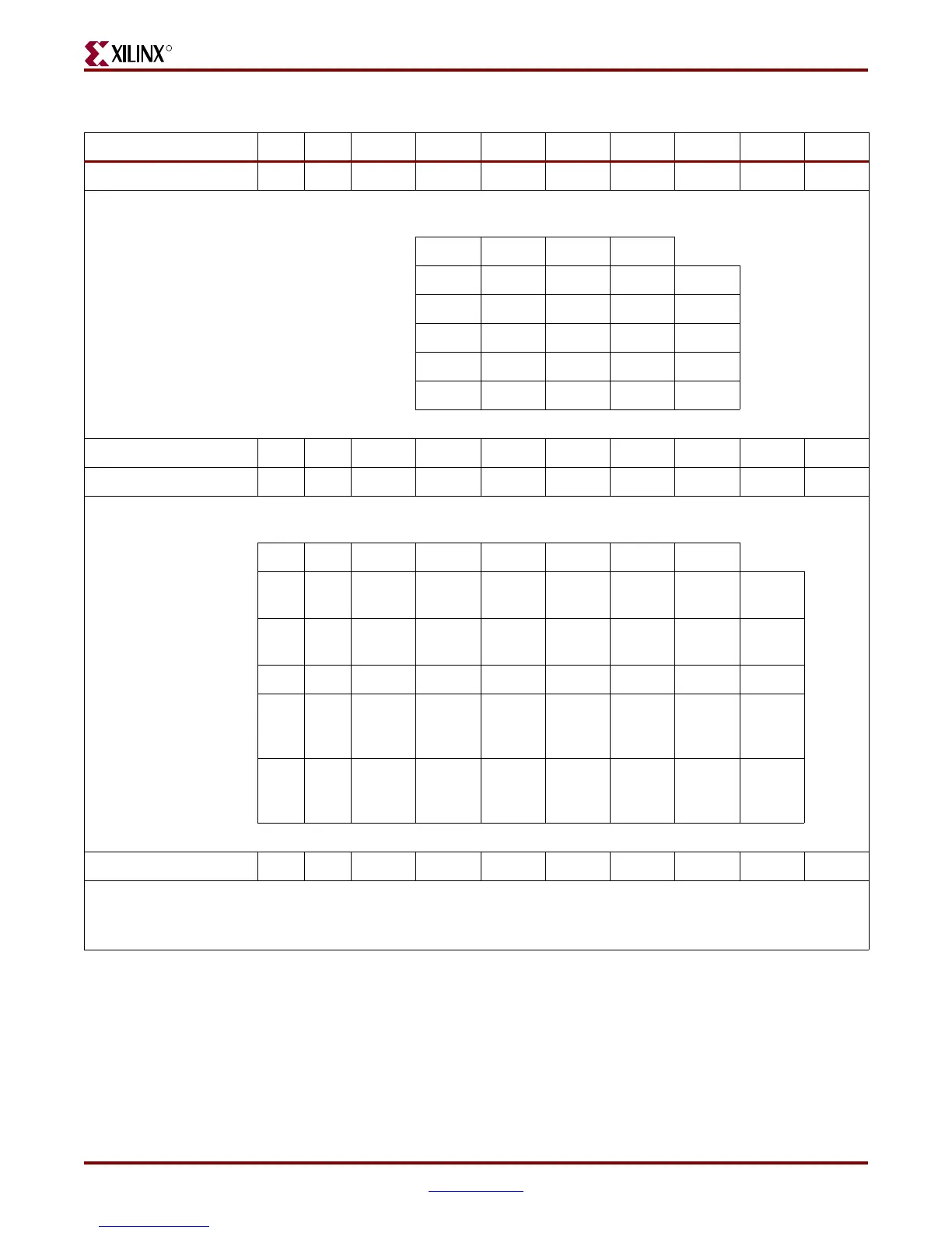
Hardware Schematic Diagram
R
Set page address 0 0 1 0 1 1 P3 P2 P1 P0
This instruction sets the address of the display data page. Any RAM data bit can be accessed when its page address and column address are
specified. Changing the Page Address does not affect the display status.
P3 P2 P1 P0
0000page 0
0001page 1
.. .. .. ..
...
0111page 7
1000page 8
Set column address MSB 0 0 0 0 0 1 Y7 Y6 Y5 Y4
Set column address LSB 0 0 0 0 0 0 Y3 Y2 Y1 Y0
This instruction sets the address of the display data RAM. When a read or write to or from the display data RAM occurs, the addresses are
automatically increased.
Y7 Y6 Y5 Y4 Y3 Y2 Y1 Y0
00000000
Col
Addr 0
00000001
Col
Addr 1
.. .. .. .. .. .. .. .. ...
11111110
Col
Addr
130
11111111
Col
Addr
131
ADC select 0 0 1 010000ADC
This instruction changes the relationship between RAM column address and segment driver.
ADC = 0, SEG1 --> SEG132 default mode
ADC = 1, SEG132 --> SEG1
Table C-6: Display Instructions (Continued)
Instruction RS RW DB7 DB6 DB5 DB4 DB3 DB2 DB1 DB0
 Loading...


