136 www.xilinx.com Virtex-5 FPGA ML561 User Guide
UG199 (v1.2.1) June 15, 2009
Appendix C: LCD Interface
R
Display Data Byte
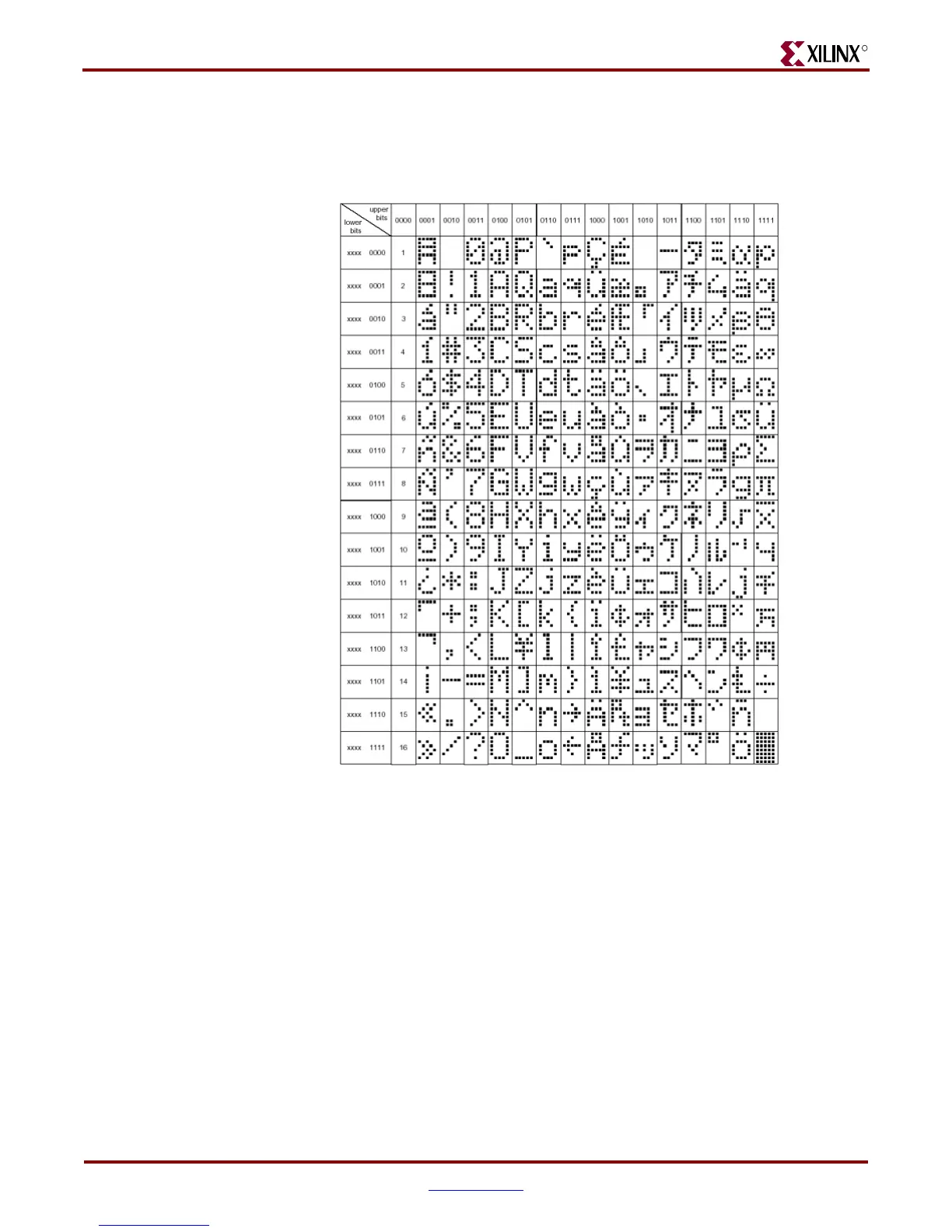
The supplied byte must be a valid ASCII representation of a character as shown in
Figure C-9.
The character set is stored in block RAM (used as ROM). The CharacterSet.xls file
contains the layout of the block RAM character set. The block RAM (see Figure C-10) is
organized as small arrays of eight bytes, which is easy for address calculation.
Figure C-9: ASCII Character Representations
UG199_C_09_050106
 Loading...


