22 www.xilinx.com Virtex-5 FPGA ML561 User Guide
UG199 (v1.2.1) June 15, 2009
Chapter 3: Hardware Description
R
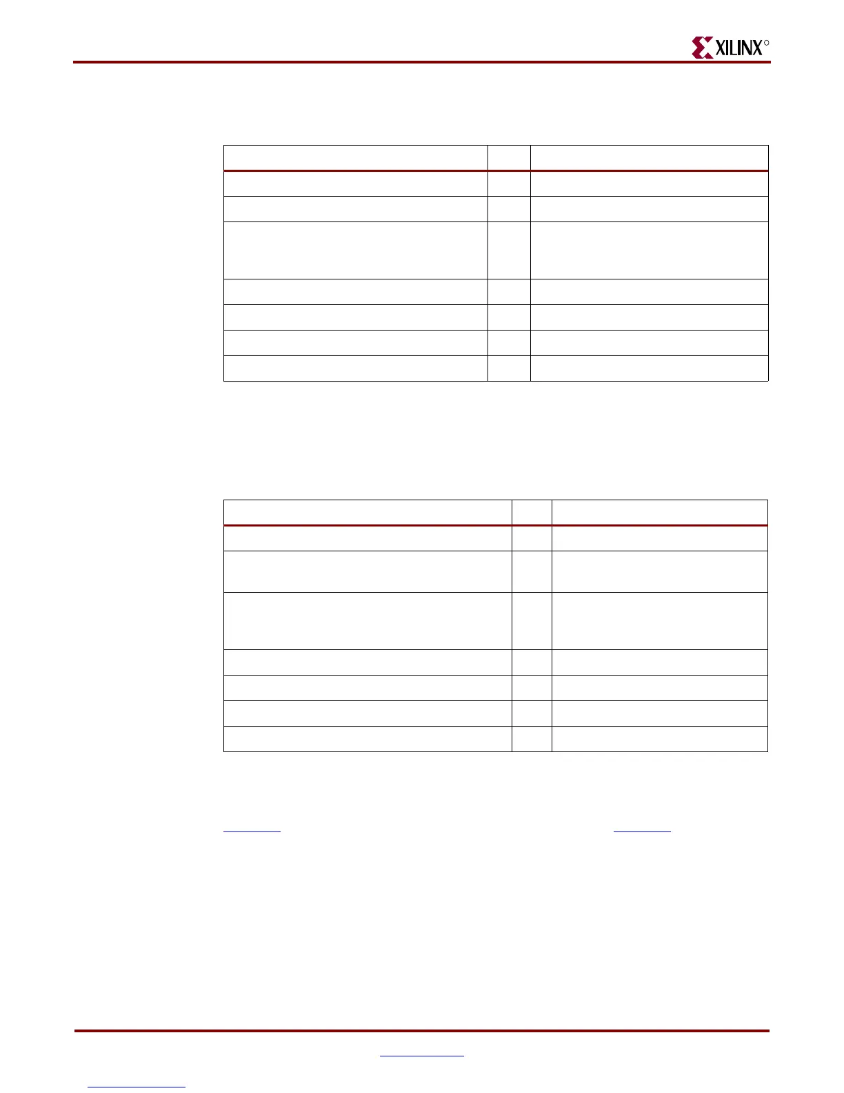
Table 3-3 describes all signals associated with DDR400 Component memories.
Table 3-4 describes all signals associated with DDR2 Component memories. For a complete
list of FPGA #1 signals and their pin locations, refer to Appendix A, “FPGA Pinouts.”
X
APP851, DDR SDRAM Controller Using Virtex-5 FPGA Devices, XAPP858, High-
Performance DDR2 SDRAM Interface in Virtex-5 Devices, and the corresponding demos are
included on the CD shipped with the ML561 Tool Kit. For a complete list of FPGA #1
signals and their pin locations, refer to Appendix A, “FPGA Pinouts.”
Table 3-3: DDR400 Component Signal Summary
Board Signal Name(s) Bits Description
DDR1_A[13:0] 14 DDR400 Component Address
DDR1_CK[2:1]_[P,N] 4 DDR400 Component Differential Clock
DDR1_[RAS,CAS,WE]_N, DDR1_CKE,
DDR1_BA[1:0], DDR1_BY[0_1,2_3]_CS_N,
DDR1_DM_BY[3:0]
12 DDR400 Component Control Signals
DDR1_DQ_BY0_B[7:0], DDR1_DQS_BY0_P 9 DDR400 Data and Strobe: Byte 0
DDR1_DQ_BY1_B[7:0], DDR1_DQS_BY1_P 9 DDR400 Data and Strobe: Byte 1
DDR1_DQ_BY2_B[7:0], DDR1_DQS_BY2_P 9 DDR400 Data and Strobe: Byte 2
DDR1_DQ_BY3_B[7:0], DDR1_DQS_BY3_P 9 DDR400 Data and Strobe: Byte 3
Notes:
1. DDR1_CKE signal has a weak 4.7KΩ pull-down resistor to meet the memory power-up requirements.
Table 3-4: DDR2 Component Signal Summary
Board Signal Name(s) Bits Description
DDR2_A[12:0] 13 DDR2 Component Address
DDR2_CK[1:0]_[P,N] 4 DDR2 Component Differential
Clock
DDR2_ODT[1:0], DDR2_[RAS,CAS,WE]_N,
DDR2_CKE, DDR2_BA[1:0], DDR2_CS[1:0]_N,
DDR2_DM_BY[3:0]
14 DDR2 Component Control Signals
DDR2_DQ_BY0_B[7:0], DDR2_DQS_BY0_[P,N] 10 DDR2 Data and Strobe: Byte 0
DDR2_DQ_BY1_B[7:0], DDR2_DQS_BY1_[P,N] 10 DDR2 Data and Strobe: Byte 1
DDR2_DQ_BY2_B[7:0], DDR2_DQS_BY2_[P,N] 10 DDR2 Data and Strobe: Byte 2
DDR2_DQ_BY3_B[7:0], DDR2_DQS_BY3_[P,N] 10 DDR2 Data and Strobe: Byte 3
Notes:
1. DDR2_CKE and DDR2_ODT[1:0] signals have a weak 4.7KΩ pull-down resistor to meet the memory
power-up requirements.
 Loading...


