24 www.xilinx.com Virtex-5 FPGA ML561 User Guide
UG199 (v1.2.1) June 15, 2009
Chapter 3: Hardware Description
R
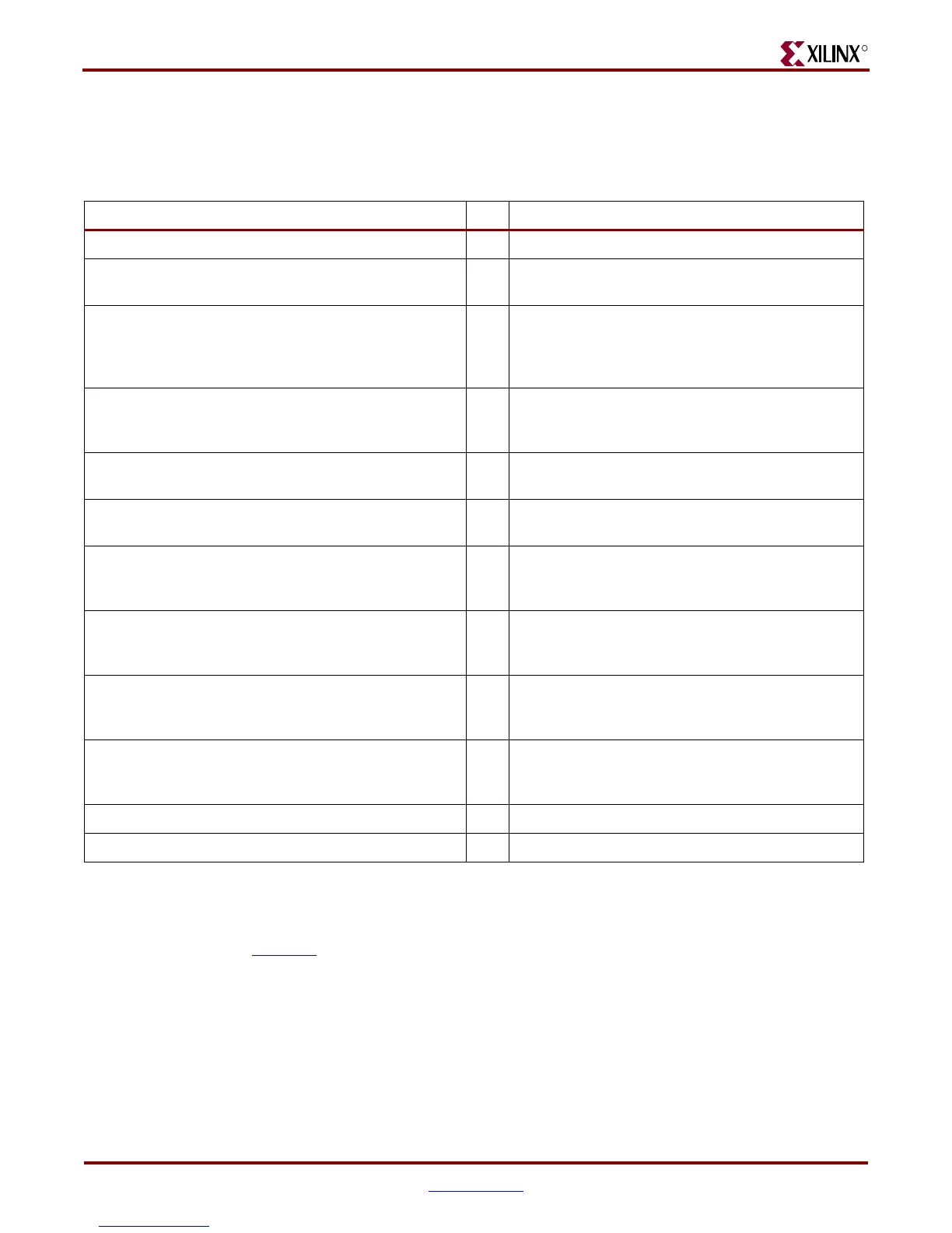
Table 3-5 describes all the signals associated with DDR2 DIMM component memories. For
the Deep DIMM interface to four DIMMs, the individual dedicated control signals are
listed at the bottom of Table 3-5.
XAPP858
, High-Performance DDR2 SDRAM Interface in Virtex-5 Devices and its
corresponding demo are included on the CD shipped with the ML561 Tool Kit.
Table 3-5: DDR2 DIMM Signal Summary
Board Signal Name(s) Bits Description
DDR2_DIMM_A[15:0] 16 DDR2 DIMM Address
DDR2_DIMM[5:1]_CK[2:0]_[P,N] 30 DDR2 DIMM Differential Clocks: Three copies per
DIMM
DDR2_DIMM_[RAS,CAS,WE,RESET]_N,
DDR2_DIMM[5:1]_CKE[1:0], DDR2_DIMM_BA[2:0],
DDR2_DIMM[5:1]_CS[1:0]_N,
DDR2_DIMM[5:1]_ODT[1:0]
37 DDR2 DIMM Common Control Signals
DDR2_DIMM[1:5]_CS[1:0]_N,
DDR2_DIMM[1:5]_CKE[1:0],
DDR2_DIMM[1:5]_ODT[1:0]
20 DDR2 DIMM Dedicated Control Signals
DDR2_DIMM_LB_BK[11,13,15]_[IN,OUT] 6 Deep DIMMs (DIMM1 through DIMM4) Loopback
Signals
DDR2_DIMM_LB_BK[12,18,20] 3 Wide DIMM (DIMM5) Loopback Signals (Total of six
FPGA pins)
DDR2_DIMM[1:5]_CNTL_PAR,
DDR2_DIMM[1:5]_CNTL_PAR_ERR,
DDR2_DIMM[1:5]_NC_019, DDR2_DIMM[1:5]_NC_102
20 Miscellaneous Place Holder Signals to the Five
DIMMs
DDR2_DIMM_DQ_BY[0:15]_B[7:0],
DDR2_DIMM_DQS_BY[0:15]_L_[P,N],
DDR2_DIMM_DM_BY[0:15]
176 DDR2 DIMM Data, Strobes, and Data Mask: Bytes 0
through 15
DDR2_DIMM_DQ_CB0_7_B[7:0],
DDR2_DIMM_DQS_CB0_7_L_[P,N],
DDR2_DIMM_DM_CB0_7
11 DDR2 DIMM Data, Strobes, and Data Mask: Check
Byte 0
DDR2_DIMM_DQ_CB8_15_B[7:0],
DDR2_DIMM_DQS_CB8_15_L_[P,N],
DDR2_DIMM_DM_CB8_15
11 DDR2 DIMM Data, Strobes, and Data Mask: Check
Byte 1
DDR2_DIMM[1:5]_SA[2:0] 15 Serial PROM Address
DDR2_DIMM_[SCL,SDA]" 2 Serial PROM interface CLK and Data
Notes:
1. DDR2_DIMM_CKE and DDR2_DIMM_ODT signals are connected to a 4.7KΩ pull-down resistor to meet the memory power-up
requirements.
 Loading...


