42 www.xilinx.com Virtex-5 FPGA ML561 User Guide
UG199 (v1.2.1) June 15, 2009
Chapter 4: Electrical Requirements
R
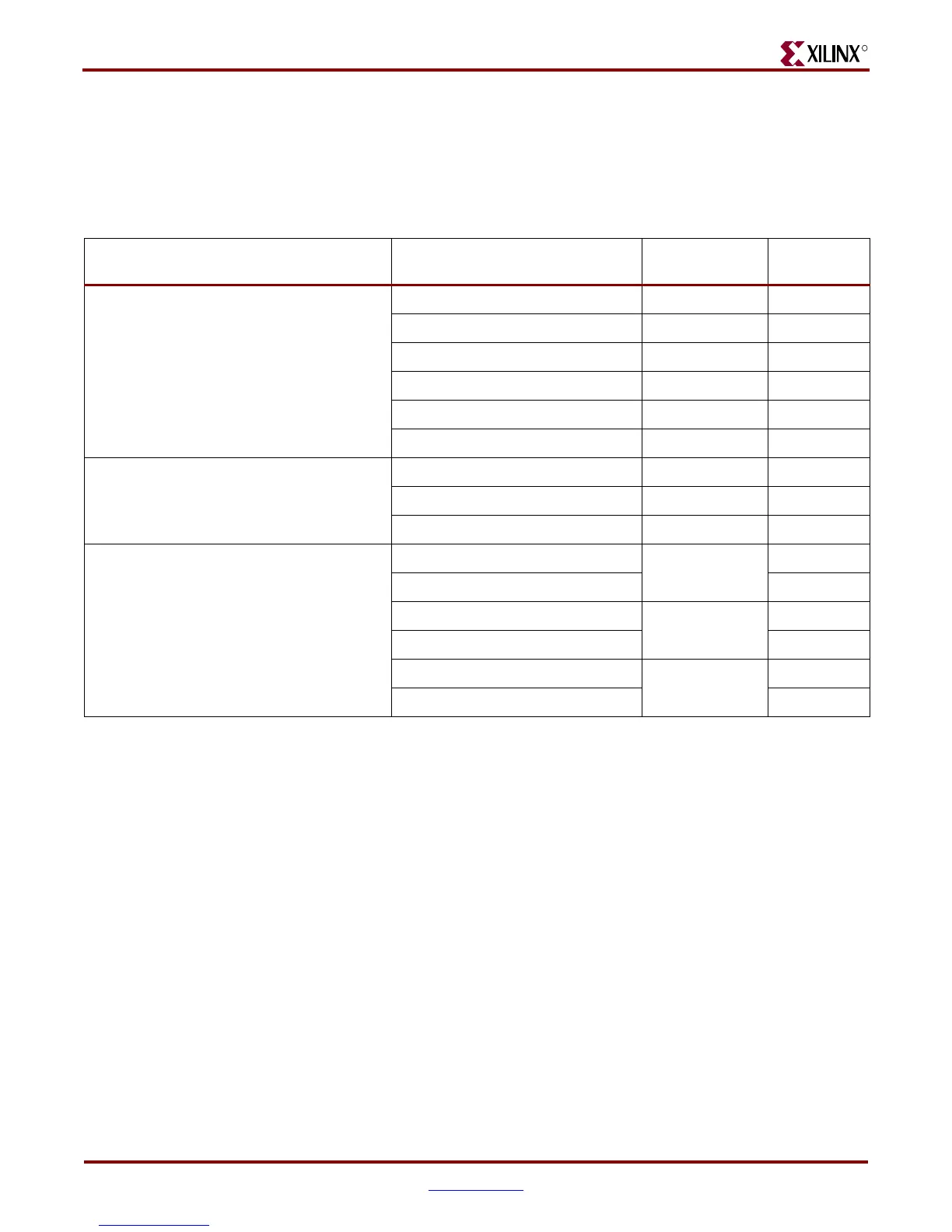
Table 4-2 lists the 12 different power planes on the Virtex-5 FPGA ML561 Development
Board. For the SSTL2, SSTL18, and HSTL power, separate power modules are
implemented for V
CCO
to FPGA, and V
DD
to memory, allowing for ease of power
measurement for the FPGAs. The power modules for V
CCO
inputs are implemented with
TI PTH05010 modules, which have provisions for ± 5% voltage margining pins.
Each of the three Fairchild FN6555 Bus Terminator Regulators has two voltage outputs:
one each for V
REF
and V
TT
. The FN6555 regulator is a push-pull device rated at ± 3A for the
V
TT
output and 3 mA for the V
REF
output.
Because the V
REF
voltage is used by the FPGA and memory devices only as reference, the
power supply does not source any real current. Thus the 3 mA capacity for the V
REF
output
is considered sufficient.
The V
TT
voltage is guaranteed to within ± 20 mV of the V
REF
output by the FN6555
regulator. The minimum driver output voltage swing around V
REF
is specified for the
SSTL18, SSTL2, and HSTL I/O standards as:
• SSTL2: ± 608 mV
• SSTL18: ± 603 mV
• HSTL: ± 500 mV (for HSTL18)
For a given memory interface, the maximum number of single-ended (non-differential)
signals that might need to be pulled up or down at a time for QDRII is 144 data bits and
approximately 30 address and control signals. The differential pair signals offset for the
sink and source of current. With a continuous current capacity of 3A for the FN6555
regulator, the regulator can supply up to (3000 / 175) = 17 mA of current per signal. The
maximum drive strength for a driver is specified at 16 mA. For a 50Ω V
TT
termination, this
Table 4-2: Power Planes
Voltage Regulator Module (VRM) Part Power Plane VRM REFDES
Stack-Up
Layer
TI PTH05010 15A Modules
V
CCINT
Power Plane (1.0V) VR6 Layer 4
SSTL18 FPGA Power Plane (1.8V) VR1 Layer 7
HSTL FPGA Power Plane (1.8V) VR10 Layer 8
V
CCAUX
Power Plane (2.5V) VR12 Layer 11
SSTL2 FPGA Power Plane (2.6V) VR9 Layer 8
TTL Power Plane (3.3V) VR13 Layer 11
TI PTH05000 6A Modules
SSTL18 Memory Power Plane (1.8V) VR4 Layer 7
HSTL Memory Power Plane (1.8V) VR14 Layer 8
SSTL2 Memory Power Plane (2.6V) VR2 Layer 8
Fairchild FN6555 3A Bus Term Regulators
(Separate outputs for V
TT
and V
REF
)
SSTL18_VREF Power Plane (0.9V)
U14
Layer 8
SSTL18_VTT Power Plane (0.9V) Layer 8
HSTL_VREF Power Plane (0.9V)
U42
Layer 7
HSTL_VTT Power Plane (0.9V) Layer 7
SSTL2_VREF Power Plane (1.3V)
U2
Layer 7
SSTL2_VTT Power Plane (1.3V) Layer 7
 Loading...


