48 www.xilinx.com Virtex-5 FPGA ML561 User Guide
UG199 (v1.2.1) June 15, 2009
Chapter 5: Signal Integrity Recommendations
R
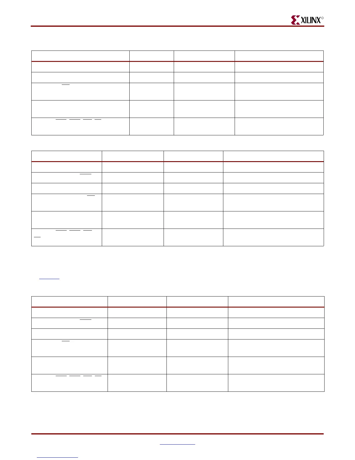
Table 5-1: DDR400 SDRAM Component Terminations
Signal FPGA Driver Termination at FPGA Termination at Memory
Data (DQ) SSTL2_II_DCI No termination 50Ω pull-up to 1.3V
Data Strobe (DQS) SSTL2_II_DCI No termination 50Ω pull-up to 1.3V
Clock (CK, CK
) SSTL2_II No termination 100Ω differential termination
between pair
Address (A, BA) SSTL2_II No termination 50Ω pull-up to 1.3V after the last
component
Control (RAS
, CAS, WE, CS, DM, and
CKE)
SSTL2_II No termination 50Ω pull-up to 1.3V after the last
component
Table 5-2: DDR2 SDRAM DIMM Terminations
Signal FPGA Driver Termination at FPGA Termination at Memory
Data (DQ) SSTL18_II_DCI No termination No termination (use 75Ω ODT
(1)
)
Data Strobe (DQS, DQS
) DIFF_SSTL18_II_DCI No termination No termination (use 75Ω ODT)
Data Mask (DM) SSTL18_II No termination No termination (use 75Ω ODT)
6 Pairs of Clocks (CK, CK
),
3 each per DIMM
SSTL18_II No termination No termination
(2)
Address (A, BA) SSTL18_II No termination 50Ω pull-up to 0.9V after the second
DIMM
Control (RAS
, CAS, WE,
CS
, CKE, and others)
SSTL18_II No termination 50Ω pull-up to 0.9V after the second
DIMM
Notes:
1. Due to use of DCI I/O for DQ and DQS, these signals have parallel termination at the source during Write operations. Simulation
results show that use of a weaker 75Ω ODT instead of a matching 50Ω ODT setting gives better noise margin at the memory.
2. The DIMM already contains 120Ω differential termination. A 5 pF capacitive termination is provided on the board as per Micron
TN-47-01
.
Table 5-3: DDR2 SDRAM Component Terminations
Signal FPGA Driver Termination at FPGA Termination at Memory
Data (DQ) SSTL18_II_DCI No termination No termination (use 75Ω ODT)
Data Strobe (DQS, DQS
) DIFF_SSTL18_II_DCI No termination No termination (use 75Ω ODT)
Data Mask (DM) SSTL18_II No termination No termination (use 75Ω ODT)
Clock (CK, CK
) SSTL18_II No termination 100Ω differential termination between
pair
Address (A, BA) SSTL18_II No termination 50Ω pull-up to 0.9V after the last
component
Control (RAS
, CAS, WE, CS,
and CKE)
SSTL18_II No termination 50Ω pull-up to 0.9V after the last
component
 Loading...


