ZC706 Evaluation Board User Guide www.xilinx.com 70
UG954 (v1.5) September 10, 2015
Feature Descriptions
• 68 single-ended or 34 differential user-defined signals
•1 GTX transceiver
•1 GTX clock
• 2 differential clocks
• 61 ground and 10 power connections
The connections between the HPC connector at J5 and AP SoC U1 implements a subset of
this connectivity:
• 34 differential user-defined pairs (34 LA pairs, LA00–LA33)
•1 GTX transceiver
•1 GTX clock
• 2 differential clocks
• 61 ground and 9 power connections
Note:
LPC FMC (J5) GA0 = GA1 = 0 = GND.
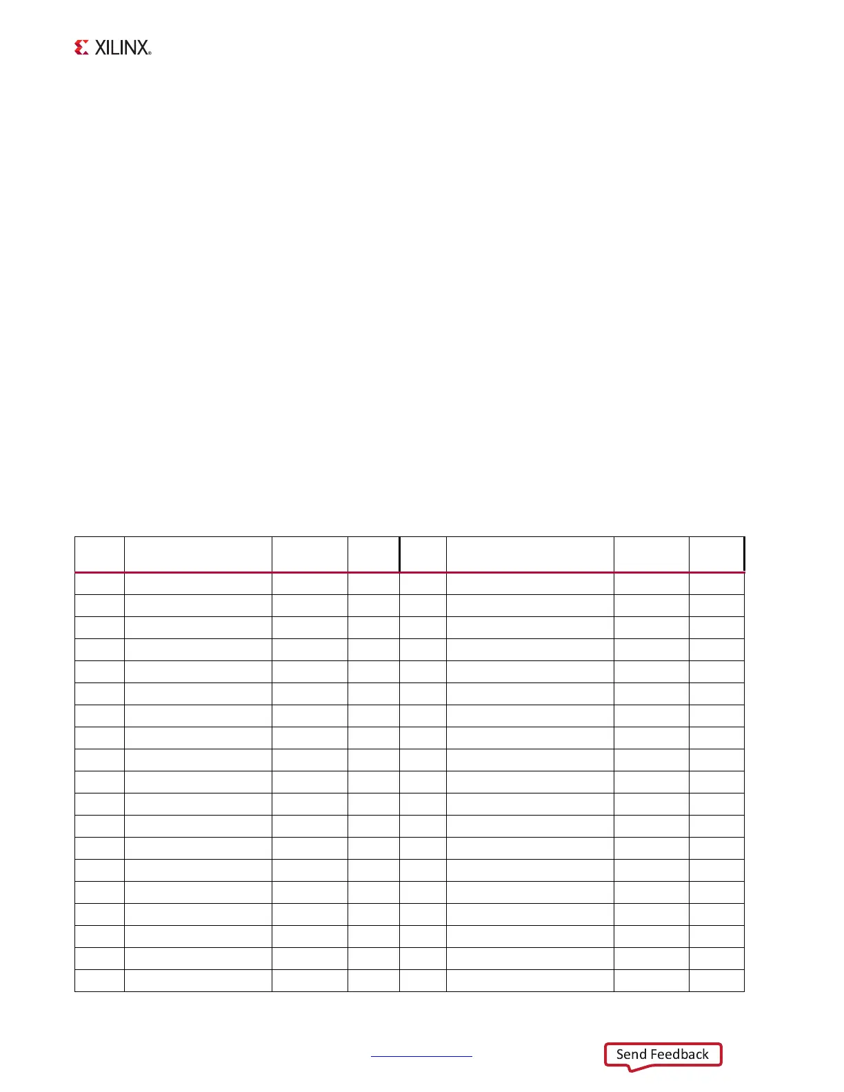
Table 1-33 shows the FMC LPC connections between J5 and XC7Z045 AP SoC U1.
Table 1-33: J5 LPC FMC Connections to AP SoC U1
J5 FMC
LPC Pin
Net Name I/O Standard
XC7Z045
(U1) Pin
J5 FMC
LPC Pin
Net Name I/O Standard
XC7Z045
(U1) Pin
C2 FMC_LPC_DP0_C2M_P
(1)
AB2 D1 PWRCTL1_FMC_PG_C2M LVCMOS25 AB20
C3 FMC_LPC_DP0_C2M_N
(1)
AB1 D4 FMC_LPC_GBTCLK0_M2C_P
(1)
U8
C6 FMC_LPC_DP0_M2C_P
(1)
AC4 D5 FMC_LPC_GBTCLK0_M2C_N
(1)
U7
C7 FMC_LPC_DP0_M2C_N
(1)
AC3 D8 FMC_LPC_LA01_CC_P LVCMOS25 AF15
C10 FMC_LPC_LA06_P LVCMOS25 AB12 D9 FMC_LPC_LA01_CC_N LVCMOS25 AG15
C11 FMC_LPC_LA06_N LVCMOS25 AC12 D11 FMC_LPC_LA05_P LVCMOS25 AE16
C14 FMC_LPC_LA10_P LVCMOS25 AC14 D12 FMC_LPC_LA05_N LVCMOS25 AE15
C15 FMC_LPC_LA10_N LVCMOS25 AC13 D14 FMC_LPC_LA09_P LVCMOS25 AH14
C18 FMC_LPC_LA14_P LVCMOS25 AF18 D15 FMC_LPC_LA09_N LVCMOS25 AH13
C19 FMC_LPC_LA14_N LVCMOS25 AF17 D17 FMC_LPC_LA13_P LVCMOS25 AH17
C22 FMC_LPC_LA18_CC_P LVCMOS25 AE27 D18 FMC_LPC_LA13_N LVCMOS25 AH16
C23 FMC_LPC_LA18_CC_N LVCMOS25 AF27 D20 FMC_LPC_LA17_CC_P LVCMOS25 AB27
C26 FMC_LPC_LA27_P LVCMOS25 AJ28 D21 FMC_LPC_LA17_CC_N LVCMOS25 AC27
C27 FMC_LPC_LA27_N LVCMOS25 AJ29 D23 FMC_LPC_LA23_P LVCMOS25 AJ26
C30 FMC_LPC_IIC_SCL N/A U65.15 D24FMC_LPC_LA23_NLVCMOS25AK26
C31 FMC_LPC_IIC_SDA N/A U65.14 D26 FMC_LPC_LA26_P LVCMOS25 AJ30
C34 GA0 = 0 = GND N/A N/A D27 FMC_LPC_LA26_N LVCMOS25 AK30
C35 VCC12_P N/A N/A D29 FMC_LPC_TCK_BUF N/A U23.14
C37 VCC12_P N/A N/A D30 FMC_HPC_TDO_FMC_LPC_TDI N/A U31.1