ZC706 Evaluation Board User Guide www.xilinx.com 84
UG954 (v1.5) September 10, 2015
Feature Descriptions
The ZC706 evaluation board supports both the internal XC7Z045 AP SoC sensor
measurements and the external measurement capabilities of the XADC. Internal
measurements of the die temperature, VCCINT, VCCAUX, and VCCBRAM are available.
Jumper J52 can be used to select either an external voltage reference (VREF) or on-chip
voltage reference for the analog-to-digital converter.
For external measurements an XADC header (J63) is provided. This header can be used to
provide analog inputs to the XC7Z045 AP SoC's dedicated VP/VN channel, and to the
VAUXP[0]/VAUXN[0], VAUXP[8]/VAUXN[8] auxiliary analog input channels. Simultaneous
sampling of Channel 0 and Channel 8 is supported.
A user-provided analog signal multiplexer card can be used to sample additional external
analog inputs using the 4 GPIO pins available on the XADC header as multiplexer address
lines. Figure 1-38 shows the XADC header connections.
Table 1-39 describes the XADC header J40 pin functions.
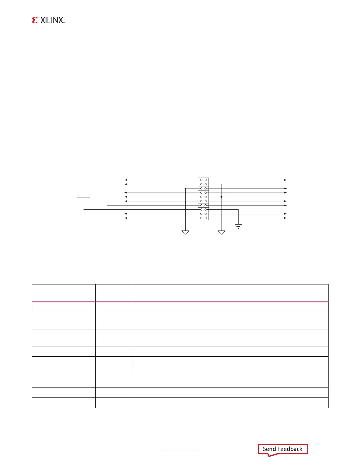
X-Ref Target - Figure 1-38
Figure 1-38: XADC Header (J63)
UG954_c1_38_041113
XADC_VP
XADC_VAUX0N
XADC_VAUX8P
XADC_DXN
XADC_VCC_HEADER
XADC_VN
XADC_VAUX0P
XADC_VAUX8N
XADC_DXP
XADC_VREF
XADC_GPIO_0
XADC_GPIO_2
XADC_GPIO_1
XADC_GPIO_3
J63
1
3
5
7
9
11
13
15
17
19
2
4
6
8
10
12
14
16
18
20
GND
XADC_AGNDXADC_AGND
XADC_VCC5V0
VCC1V5_PL
Table 1-39: XADC Header J63 Pinout
Net Name
J63 Pin
Number
Description
VN, VP 1, 2 Dedicated analog input channel for the XADC.
XADC_VAUX0P, N 3, 6
Auxiliary analog input channel 0. Also supports use as I/O inputs when anti
alias capacitor is not present.
XADC_VAUX8N, P 7, 8
Auxiliary analog input channel 8. Also supports use as I/O inputs when anti
alias capacitor is not present.
DXP, DXN 9, 12 Access to thermal diode.
XADC_AGND 4, 5, 10 Analog ground reference.
XADC_VREF 11 1.25V reference from the board.
XADC_VCC5V0 13 Filtered 5V supply from board.
XADC_VCC_HEADER 14 Analog 1.8V supply for XADC.
VCC1V5_PL 15 VCCO supply for bank which is the source of DIO pins.