ZCU102 Evaluation Board User Guide www.xilinx.com 35
UG1182 (v1.2) March 20, 2017
Chapter 3: Board Component Descriptions
The connections between the USB 2.0 PHY at U116 and the XCZU9EG MPSoC are listed in
Table 3-8.
Note that the shield for the USB 3.0 micro-B connector (J96) can be tied to GND by a jumper
on header J96 pins 2-3 (default). The USB shield can optionally be connected through a
capacitor to GND by installing a capacitor (body size 0402) at location C887 and jumping
pins 1-2 on header J112.
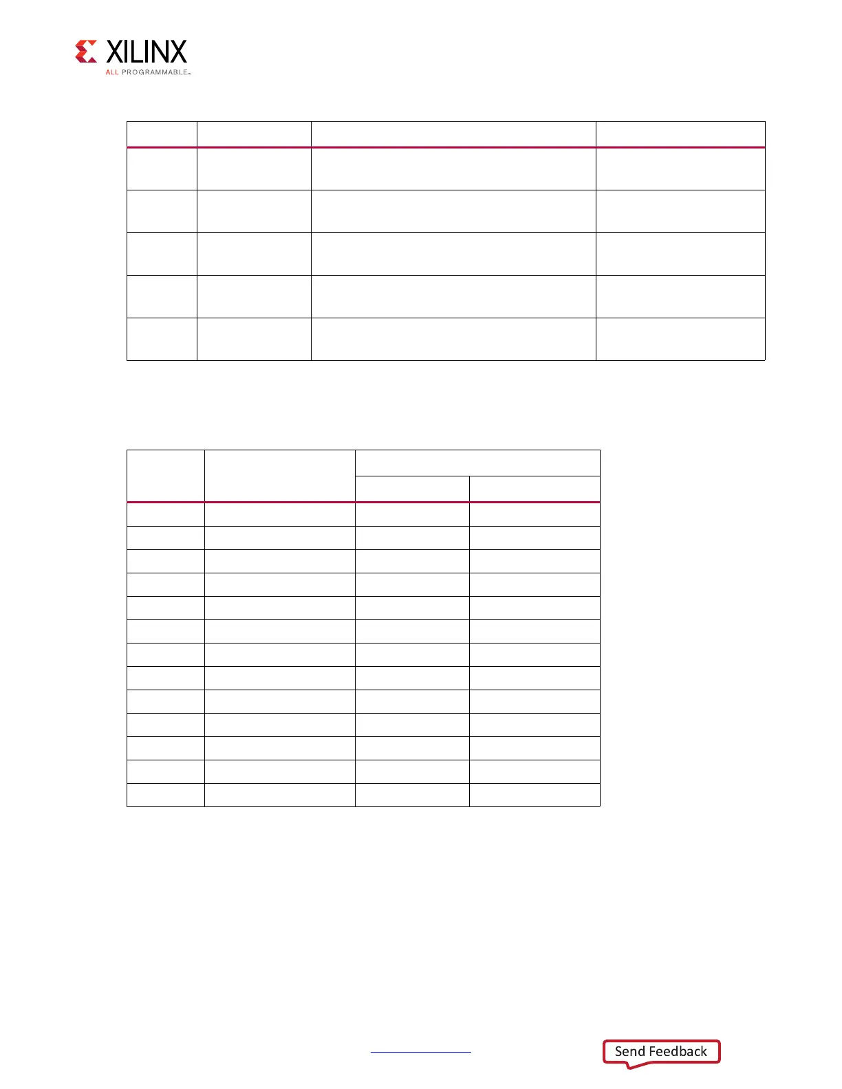
Table 3-7: USB Jumper Settings
Header Function Shunt Position Notes
J7
V
BUS
5V supply Shunt ON = Host or OTG mode
Shunt OFF = Device mode
J113
RV
BUS
select Position 1-2 = Device mode (10 kΩ)
Position 2-3 = OTG mode (1 kW)
Over voltage protection.
J110
CV
BUS
select Position 1-2 = OTG and Device mode (1 mF)
Position 2-3 = Host mode (120 µF)
V
BUS
load capacitance.
J109
Cable ID select Position 1-2 = A/B cable detect
Position 2-3 = ID not used
Used in OTG mode.
J112
USB Micro-B Position 1-2 = Shield connected to GND
Position 2-3 = Shield floating
Table 3-8: USB 2.0 ULPI Transceiver Connections to the XCZU9EG MPSoC
XCZU9EG
(U1) Pin
Net Name
USB3320 U116
Pin Number Pin Name
U117.4
(1)
ULPI0_RST_B 27 RESET_B
G23 MIO58_USB_STP 29 STP
E23 MIO53_USB_DIR 31 DIR
F22 MIO52_USB_CLK 1 CLKOUT
B23 MIO55_USB_NXT 2 NXT
C23 MIO56_USB_DATA0 3 DATA0
A23 MIO57_USB_DATA1 4 DATA1
F23 MIO54_USB_DATA2 5 DATA2
B24 MIO59_USB_DATA3 6 DATA3
E24 MIO60_USB_DATA4 7 DATA4
C24 MIO61_USB_DATA5 9 DATA5
G24 MIO62_USB_DATA6 10 DATA6
D24 MIO63_USB_DATA7 13 DATA7
Notes:
1. PS_POR_B (U1.V23) or PS_MODE1 (DIP SW6.2) or PB SW2 drive U116 RST_B via OR
gate U117.