EasyManuals Logo

Xilinx ZCU102 User Manual

Xilinx ZCU102
137 pages
To Next Page IconTo Next Page
To Previous Page IconTo Previous Page
Page #73 background imageLoading...
Page #73 background image
ZCU102 Evaluation Board User Guide www.xilinx.com 73
UG1182 (v1.2) March 20, 2017
Chapter 3: Board Component Descriptions
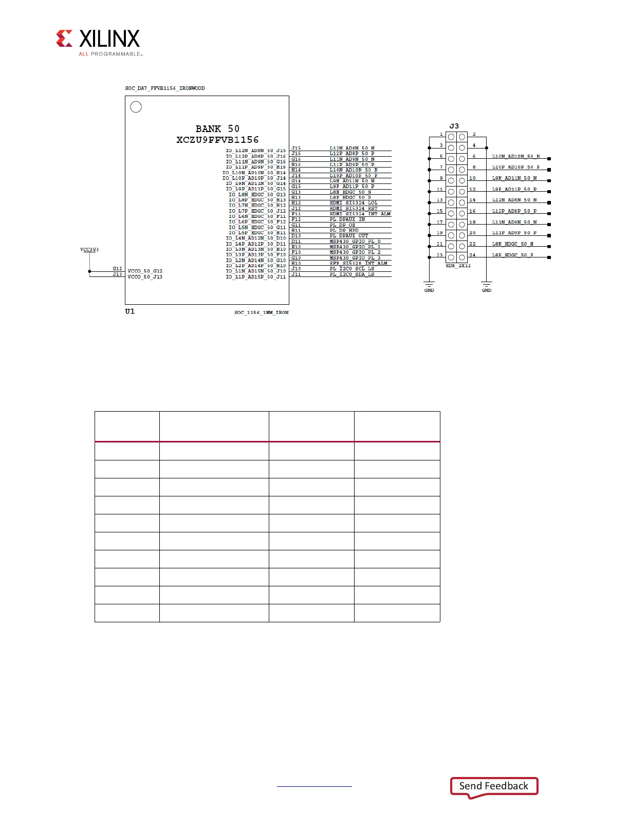
The J3 connector to MPSoC connections are listed in Table 3-32.
X-Ref Target - Figure 3-29
Figure 3-29: Prototype Header J3
Table 3-32: Prototype Header J3 Connections to the XCZU9EG MPSoC
XCZU9EG
(U1) Pin
Schematic Net Name I/O Standard
Prototype
Header J3 Pin
J15
L12N_AD8N_50_N
LVCMOS33 14
J16
L12N_AD8P_50_P
LVCMOS33 16
G16
L11N_AD9N_50_N
LVCMOS33 18
H16
L11N_AD9P_50_P
LVCMOS33 20
H14
L10N_AD10N_50_N
LVCMOS33 6
J14
L10N_AD10P_50_P
LVCMOS33 8
G14
L9N_AD11N_50_N
LVCMOS33 10
G15
L9N_AD11P_50_P
LVCMOS33 12
G13
L8N_HDGC_50_P
LVCMOS33 22
H13
L8N_HDGC_50_N
LVCMOS33 24
Send Feedback

Table of Contents

Other manuals for Xilinx ZCU102

Questions and Answers:

Question and Answer IconNeed help?

Do you have a question about the Xilinx ZCU102 and is the answer not in the manual?

Xilinx ZCU102 Specifications

General IconGeneral
ProcessorQuad-core ARM Cortex-A53, Dual-core ARM Cortex-R5
SD CardMicroSD card slot
Video OutputsDisplayPort
FPGAXilinx Zynq UltraScale+ XCZU9EG-2FFVB1156E
Memory4GB DDR4 Component Memory
StorageMicroSD card slot
EthernetGigabit Ethernet
USB1 x USB 3.0, 1 x USB 2.0
PCIePCIe Gen2 x4
DisplayDisplayPort
Power Supply12V DC input
SATASATA 3.0
ClockingProgrammable clocks
Operating System SupportPetaLinux

Related product manuals