A
1
2
3
4
5
6
7
8
9
10
BCDEFGH I JK
L MN
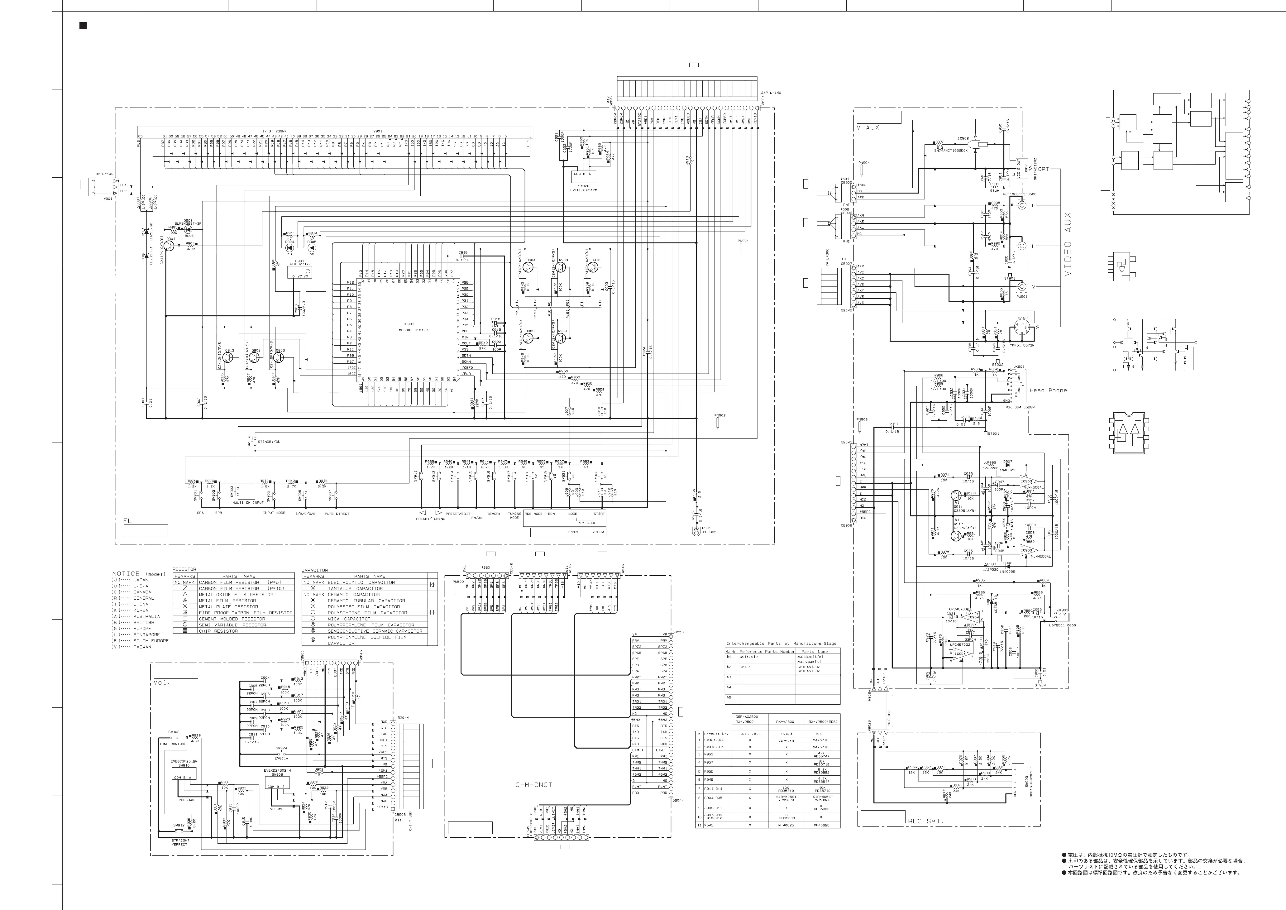
RX-V2500/DSP-AX2500
SCHEMATIC DIAGRAM (OPERATION)
75
★ All voltages are measured with a 10MΩ/V DC electronic volt meter.
★ Components having special characteristics are marked s and must be replaced
with parts having specifications equal to those originally installed.
★ Schematic diagram is subject to change without notice.
FL DRIVER
-23.7
-22.9
-20.7
-20.8
-24.8
-16.6
-16.6
-17.7
-16.5
-22.7
-16.8
-28.8
-14.8
-12.6
-24.8
-18.7
-24.8
-12.8
-16.7
-20.5
-16.5
-20.1
-12.8
-12.9
-26.9
-24.8
-26.8
-8.7
-16,7
-24.7
-28.8
-30.9
-8.7
-14.5
-16.8
-10.7
-12.8
-12.5
-24.8
-26.9
-12.9
-12.9
-16.5
-16.5
-20.6
-16.7
-12.8
-24.8
-18.7
-24.8
-12.6
-14.8
5.0
-28.8
5.0
2.2
2.2
5.0
5.0
0
0
0
-16.8
5.0
-20.6
-20.6
-20.0
-20.1
-12.8
-12.5
-12.9
-12.9
-12.9
-12.8
5.0 5.0
5.0 5.0
-22.7
-16.5
-12.7
-16.6
-16.6
-24.6
-20.8
-29.0
-29.0
-29.1
-29.0
-29.0
-29.0
-29.0
-29.0
-29.0
-29.0
-29.0
-29.0
-28.9
-29.0
-29.0
-29.0
-29.0
-23.7
-24.0-27.6-31.3
3.0
0 5.1 5.0
3.0
0
0
5.1
5.1 5.1
5.1
-28.7 -28.8 -28.6
-28.9 -28.9 -29.1
-20.7
-22.9
-28.7
-28.8
-28.8
-29.0
-29.0
-29.0
-29.0
-29.0
-29.0
-29.0
-29.0
-29.0
-28.9
-29.0
-29.0
-29.0
-29.0
-31.3
-26.8
-8.6
-16.7
-24.7
-28.8
-30.9
-8.7
-12.9
-16.8
-10.7
-12.8
-12.5
5.0
5.0
0
0
0
0
0
0
0
0
0
0
0
5.1
0
0
11.8
-12.0
0
0
0
0
11.8 9.3
9.3
9.6
0
0.7
0.7
0
0
-9.6
-12.0
B, G models only
U, C, A models only
1
2
3
4
5
1
8
3
2
7
4
6
5
IC901: M66003-0101FP
FL Display Driver
IC902: SN74AHCT1G32DCKR
2-Input or Gate
IC903: NJM4556AL
Dual OP-Amp
IC904: µPC4570G2
Dual OP-Amp
52
Display
controller
Segment
digit
select/
output
circuit
Serial
receive
circuit
Digit
output
circuit
Clock
generator
DIG11/
SEG42
51
DIG12/
SEG41
50
DIG13/
SEG40
49
DIG14/
SEG39
48
DIG15/
SEG38
47
DIG16/
SEG37
46
DIG17/
SEG36
45
SEG35
XOUT
6
Vcc1
8
Vcc2
18
Vss
5
Vp
64
XIN
7
CS
SCK
3
SDATA
4
RESET
1
SEG00
44
9
SEG34
SEG26
17
19
SEG25
Segment
output
circuit
Display code
RAM
(8-bit x 60)
CGROM
(35 bit x 166)
CGROM
(35 bit x 16)
code
select
Code
write
Code/
command
control
circuit
DIG00
63
53
DIG10
2
data
timing
clock
dot data
write
scan pulse
Y4
B2
GND 3
Vcc5A1
8
2, 6
3, 5
1, 7
4
V+
–INPUT
+INPUT
V–
OUTPUT
–+
OUT1
–IN1
–VCC
+VCC
OUT2
1
2
3
4
5
+IN1 –IN2
+IN2
–+
6
7
8
OPE (1)
OPE (3)
OPE (2)
OPE (5)
OPE (4)
O : USED / APPLICABLE
X : NOT USED
Page 77
to POWER (2)_CB125
B9
Page 71
to DSP_W501
D1
Page 80
to CONTROL_W502
H8Page 80
to CONTROL_CB516
I8
Page 80
to CONTROL_CB508
H6
Page 76
to MAIN (1)_W220
D7
Page 77
to POWER (1)_CB41
A5
Page 77
to POWER (7)_CB131
G2 Page 74
to FUNCTION (3) – C-F_CNCT –
CB527
B7
Page 80
to CONTROL_CB514
H7
Page 80
to CONTROL_CB507
H7
Page 80
to CONTROL_CB506
I5
U, C, A, B, G models only
 Loading...