ABCDEFGH
1
2
3
4
5
6
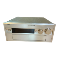
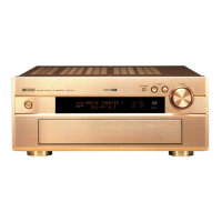
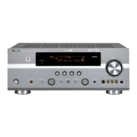
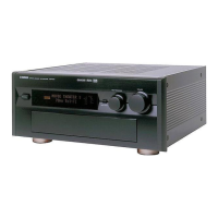
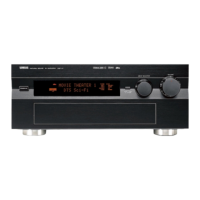
DSP-AX620
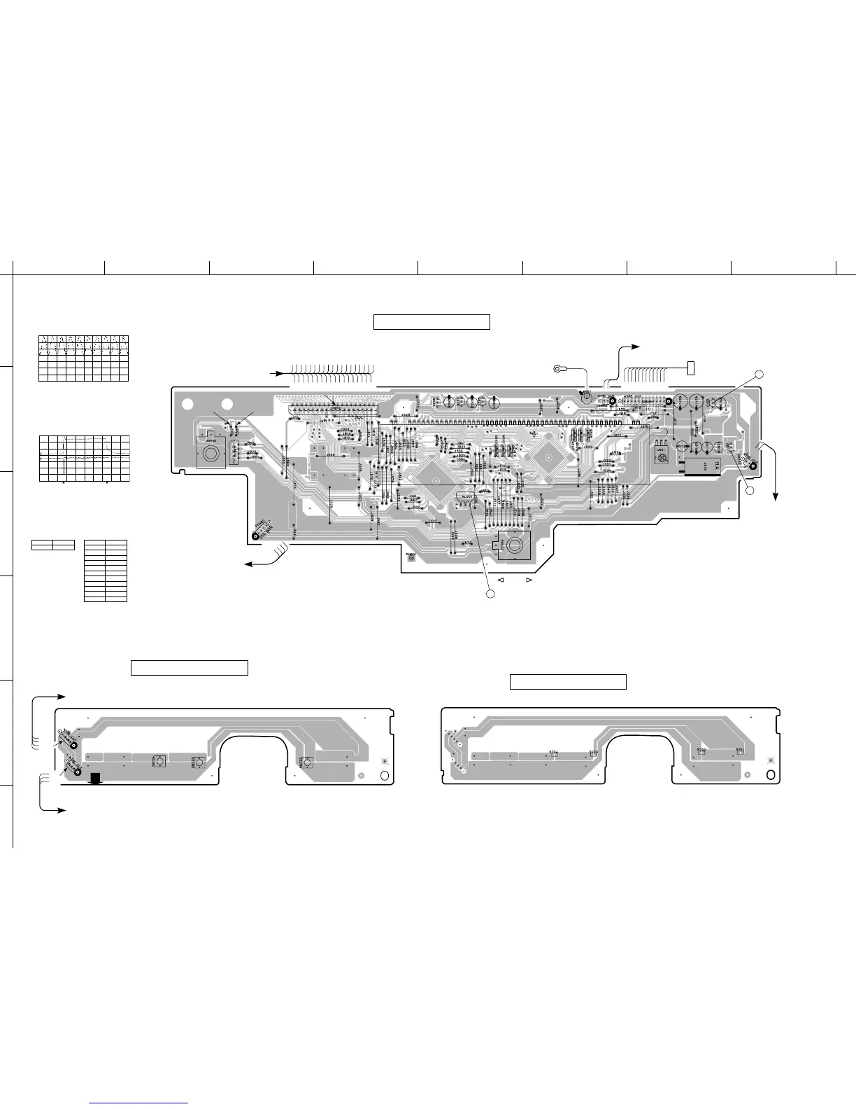
■ PRINTED CIRCUIT BOARD (Foil side)
E-54/J-52 E-55/J-53
CKP
CES
E/I
DEST
SDRR
SDTP
SDRP
/ST
INT928
MG
YSSCK
/ICD
SCN
MTC
VMT
SO
CET
PRV2
LC2
SCKR
SDTR
VSY
RDSE
CEP
SCKP
TMT
TUNED
SDD
SDM
CSY
DMT
MTSW
MTMR
CEV
SCK
CEL
LC1
FROM : INPUT (1)
VOLUME
J, B, G only J only
2
3A
3B
TO : OPE (4)
W503
MG
ADKEY2
ADKEY1
+5M
ERY
PRV1
VP
PRD
PRI
MRY
S12
PRY
MG
PREMT
HPRY
/HP
TO : MAIN (1)
W505
#505
F1
F2
TO : OPE (9)
TO : OPE (8)
+5M
PSW
W502
W501
BL
OPERATION ( 1 ) P. C. B.
(Lead Type Device)
EFFECT DSP
PROGRAM
SET MENU
MG
ADKEY2
+5M
TO : OPE (4)
W701
MG
ADKEY2
ADKEY1
+5M
TO : OPE (1)
W503
OPERATION ( 4 ) P. C. B. (Lead Type Device)
OPERATION ( 4 ) P. C. B.
(Surface Mount Device)
Point e-A (/RES : Collector of Q510)
Point e-B (S12 : Emitter of Q511)
V : 5V/div (S12), V : 2V/div (/RES)
DC, 1 : 1 probe, H : 1 sec/div
0V
0V
S12
/RES
AC CORD ON
AC CORD OFF
Point w (Pin 38 of IC501)
V : 2V/div, H : 0.1 µsec/div
DC, 1 : 1 probe
0V
Ref. No. Location
IC503 G3
● Semiconductor Location
Ref. No. Location
Q501 E2
Q502 E2
Q503 E2
Q504 E2
Q505 E2
Q506 E2
Q507 F2
Q508 F2
Q509 F2
Q510 G2
Q511 G2
 Loading...