ZYNQ FPGA Development Board AX7021 User Manual
l
Amazon Store: https://www.amazon.com/alinx
Pin Assignment:
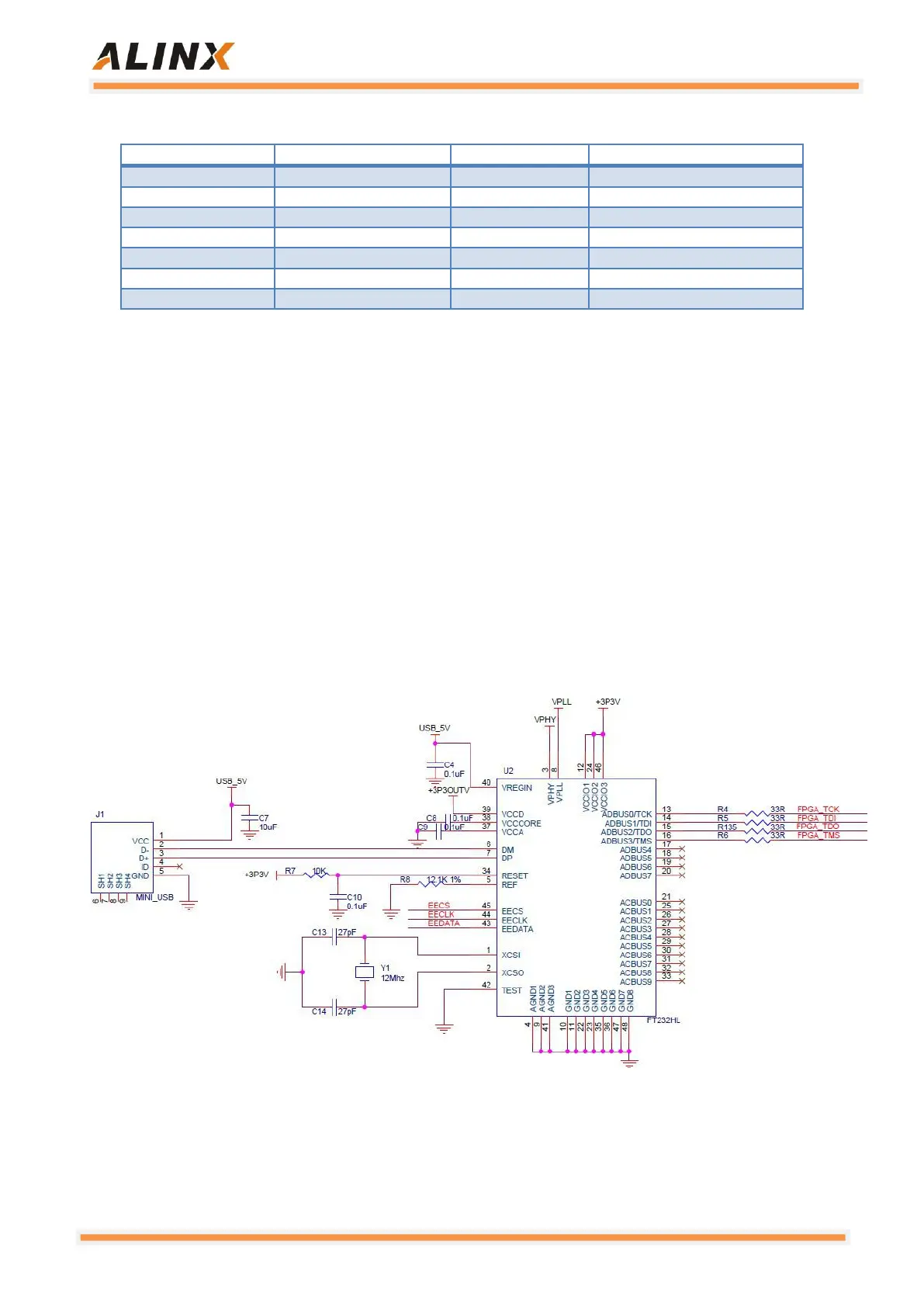
3.7 JTAG Interface
JTAG's download debug circuitry has been integrated on the AX7021
carrier board, so users do not need to purchase an additional Xilinx downloader.
As long as a USB cable can be used for ZYNQ development and debug. The
USB of PC and ZYNQ JTAG debug signals TCK, TDO, TMS, TDI are used for
data communication via the FTDI USB bridge chip FT232HL on the
development board. On the AX7021 development board, the JTAG interface is
in the USB interface mode. Users can connect the PC and JTAG interface to
the ZYNQ system debugging through the USB cable provided by us.
Figure 3-7-1: JTAG interface part of the schematic