ZYNQ FPGA Development Board AX7021 User Manual
l
Amazon Store: https://www.amazon.com/alinx
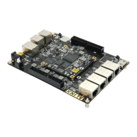
USB Interface
1 JTAG debug interface, using MINI USB interface, users can debug and
download ZYNQ system through USB cable and onboard JTAG circuit.
LED Light
9 LEDs, include 6 on the core board and 3 on the extension board. There
are 1 power indicator, 1 DONE configuration indicator, 2 user indicators and 2
serial port transceiver indicators on the core board. There are 1 power indicator
and 2 user indicators on the extension board.
Button
3 buttons, 1 reset button on the core board, and 2 user buttons on the
extension board.
Part 2: AC7021 Core Board
2.1 Introduction
The AC7021 (core board model, the same below) core board is an FPGA
development board based on the Zynq chip XC7Z020-2CLG484I of the XILINX
ZYNQ7000 series. The ZYNQ chip's PS system integrates two ARM CortexTM-
A9 processors, AMBA® interconnects, internal memory, external memory
interfaces and peripherals. The ZYNQ FPGA chip contains a wide range of
programmable logic cells, DSP and internal RAM.
The core board uses two SK Hynix DDR3 chips (H5TQ4G63AFR-PBI),
each with a 4Gbit DDR capacity; two DDR chips form a 32-bit data bus width,
and the read and write data clock frequency between ZYNQ FPGA and DDR3
is up to 533Mhz; such a configuration can meet the system's high bandwidth
data processing needs
In order to connect to the carrier board, the four board-to-board connectors
of the core board extend the USB interface of the PS side, the Gigabit Ethernet
interface, the SD card interface and other remaining MIO ports. As well as
almost all IO ports (198) of BANK13, BANK33, BAN34 and BANK35 on the PL
side, the level of IO of BANK33 and BANK34 can be modified by replacing the