ZYNQ FPGA Development Board AX7021 User Manual
l
Amazon Store: https://www.amazon.com/alinx
PS Clock pin assignment:
Table 2-6-1: PS Clock pin assignment
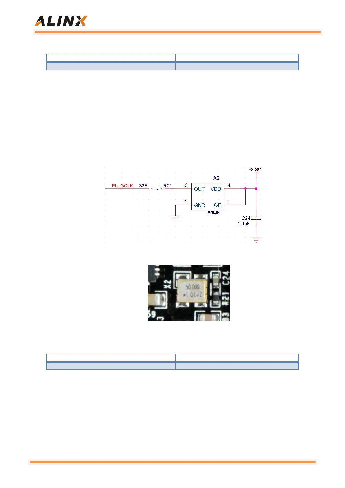
PL system clock source
The AC7021 core board provides a single-ended 50MHz PL system clock
source with 3.3V power supply. The crystal output is connected to the global
clock (MRCC) of the FPGA BANK13, which can be used to drive user logic
within the FPGA. The schematic diagram of the clock source is shown in Figure
2-6-3:
Figure 2-6-3: PL system clock source
Figure 2-6-4: 50Mhz active crystal oscillator on the Core Board
PL Clock pin assignment:
Table 2-6-2: PL Clock pin assignment
2.7 USB to serial port
For the AC7021 core board to work and debug separately, we have a Uart
to USB interface for the core board. Used for separate power supply and
debugging of the core board. The conversion chip uses the USB-UART chip of
Silicon Labs CP2102GM. The USB interface uses the MINI USB interface. It