ZYNQ FPGA Development Board AX7021 User Manual
l
Amazon Store: https://www.amazon.com/alinx
Table of Contents
Version Record
...............................................................................................................
2
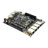
Part 1: FPGA Development Board Introduction
.....................................................
6
Part 2: AC7021 Core Board
.......................................................................................
8
2.1 Introduction........................................................................................................ 8
2.2 ZYQN Chip
......................................................................................................
10
2.3 DDR3 DRAM
...................................................................................................
13
2.4 QSPI Flash...................................................................................................... 16
2.5 eMMC Flash
....................................................................................................
17
2.6 Clock configuration
.........................................................................................
19
2.7 USB to serial port
...........................................................................................
20
2.8 LED
...................................................................................................................
22
2.9 Reset button
....................................................................................................
23
2.10 JTAGE Interface
...........................................................................................
24
2.11 DIP switch configuration
.............................................................................
25
2.12 Power
.............................................................................................................
25
2.13 Structure diagram
.........................................................................................
28
2.14 Connector pin definition
..............................................................................
28
Part 3: Carrier Board
.................................................................................................
35
3.1 Introduction
......................................................................................................
35
3.2 Gigabit Ethernet interface............................................................................. 36
3.3 USB2.0 Host interface
...................................................................................
40
3.4 HDMI Output Interface
...................................................................................
42
3.5 USB to serial port........................................................................................... 44
3.6 SD card slot
.....................................................................................................
45
3.7 JTAG Interface................................................................................................46
3.8 LED
...................................................................................................................
47
3.9 User Button
......................................................................................................
48
3.10 Extension Port.............................................................................................. 49