ZYNQ FPGA Development Board AX7021 User Manual
l
Amazon Store: https://www.amazon.com/alinx
Figure 2-9-1: Reset button connection diagram
Figure 2-9-2: Reset Button on the Core Board
Reset Pin Assignment:
Table 2-9-1: Reset Pin Assignment
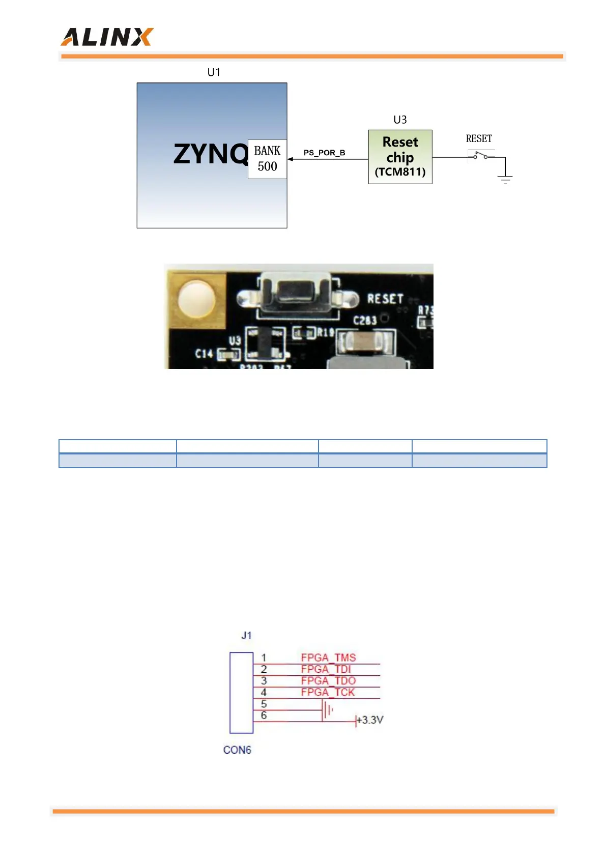
2.10 JTAGE Interface
The JTAG test socket J1 is reserved on the AC7021 core board for
separate JTAG download and debugging of the core board. Figure 2-10-1 is the
schematic part of the JTAG port, which involves TMS, TDI, TDO, TCK, GND. ,
+3.3V these six signals.
Figure 2-10-1: JTAG interface part of the core board schematic