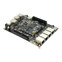
ZYNQ FPGA Development Board AX7021 User Manual
l
Amazon Store: https://www.amazon.com/alinx
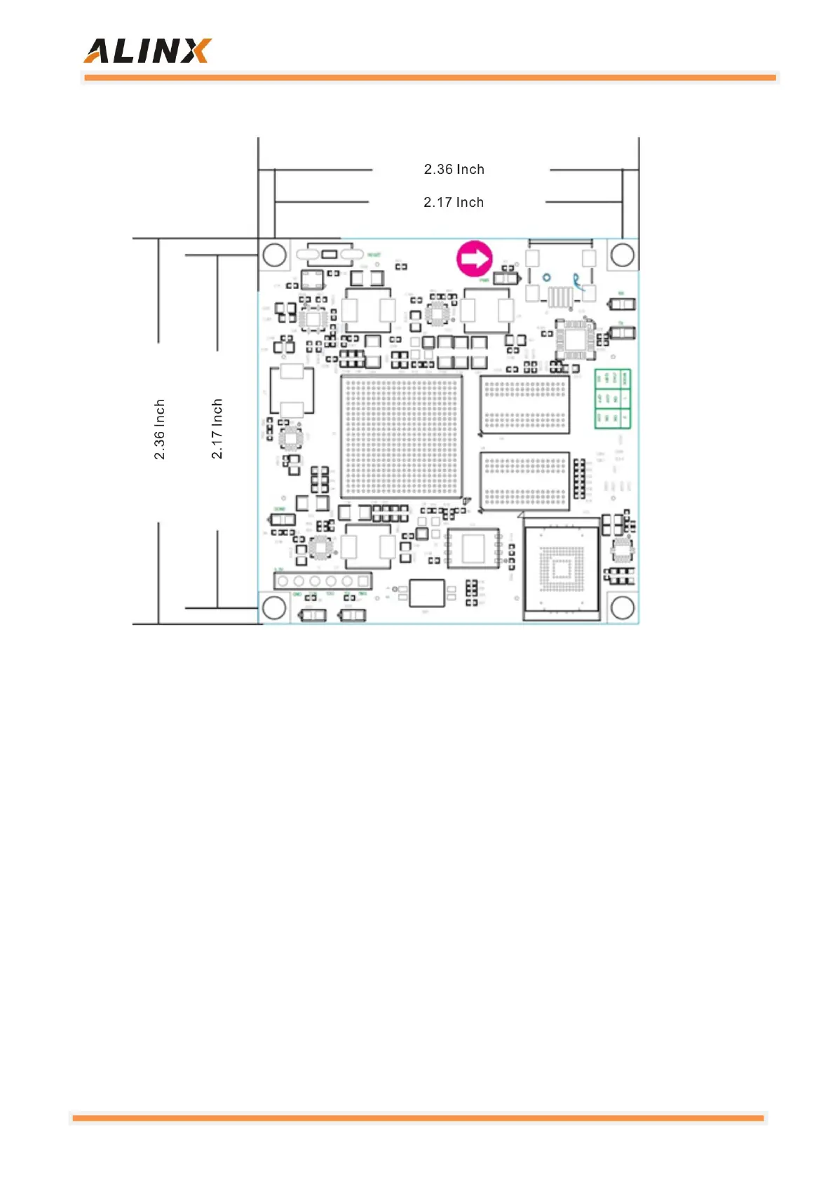
2.13 Structure diagram
Figure 2-13-1: The Structure diagram (Top View)
2.14 Connector pin definition
The core board expands four high-speed carrier ports, and uses four 80Pin
inter-board connectors (CON1~CON4) to connect with the backplane. The PIN
pitch of the connector is 0.5mm. Among them, CON1 is connected to the power
input, the MIO signal of the PS and the JTAG signal, and CON2~CON4 are
connected to the IO signals of BANK13, BANK33, BANK34, BANK35 of PL.
The IO levels of BANK33 and BANK34 can be changed by changing the level
of the LDO chip (U12) on the board. The default is 3.3V. Pin assignment
detailed as Table 2-14-1, Table 2-14-2, Table 2-14-3, Table 2-14-4: