ZYNQ FPGA Development Board AX7021 User Manual
l
Amazon Store: https://www.amazon.com/alinx
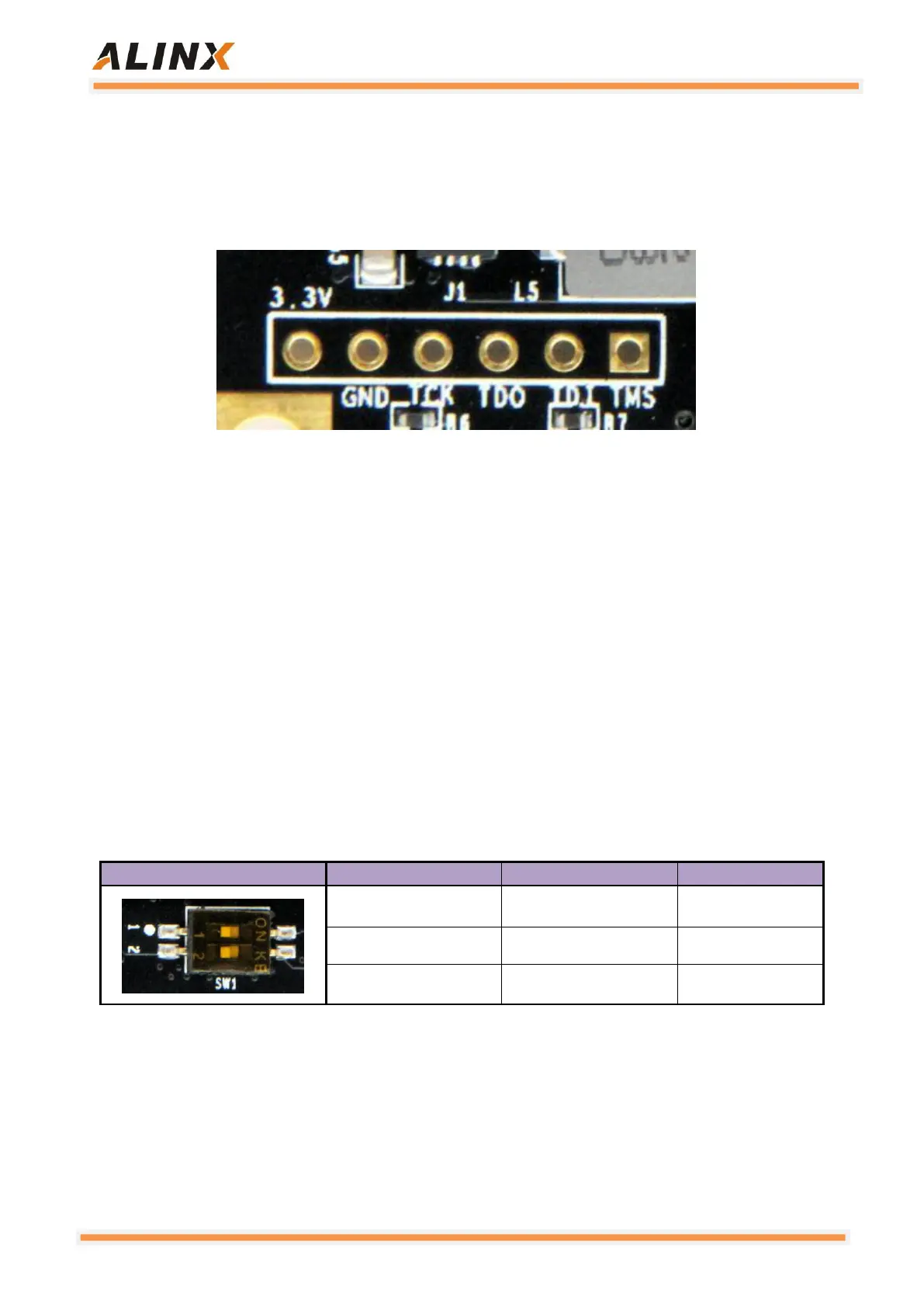
The JTAG interface J1 on the core board uses a 6-pin 2.54mm pitch
single-row test hole. If you need to use the JTAG connection to debug on the
core board, you need to solder a 6-pin single-row pin header. Figure 2-10-2
shows the physical map of the JTAG interface on the development board.
Figure 2-10-2: JTAG interface on the core board
2.11 DIP switch configuration
The AC7021 has a 2-digit DIP switch SW1 on the core board to configure
the ZYNQ system's startup mode. The AC7021 system development platform
supports three startup modes. The three startup modes are JTAG debug mode,
QSPI FLASH and SD card boot mode. After the XC7Z020 chip is powered up, it
will detect the level of the MIO port (MIO5 and MIO4) to determine which
startup mode. Users can select different startup modes through the DIP switch
SW1 on the core board. The SW1 startup mode configuration is shown in Table
2-11-1
Table 2-11-1: The SW1 Startup Mode Configuration
2.12 Power
The AC7021 core board is powered by DC5V. It is powered by the Mini
USB interface when it is used alone. It is powered by the extension board when
the backplane is connected. Please be careful not to supply power to the Mini