ZYNQ FPGA Development Board AX7021 User Manual
l
Amazon Store: https://www.amazon.com/alinx
Pin Assignment of eMMC Flash
Table 2-5-2: Pin Assignment of eMMC FLASH
2.6 Clock configuration
The AC7021 core board provides active clocks for the PS system and the
PL logic sections, respectively, so that the PS system and the PL logic can
work independently.
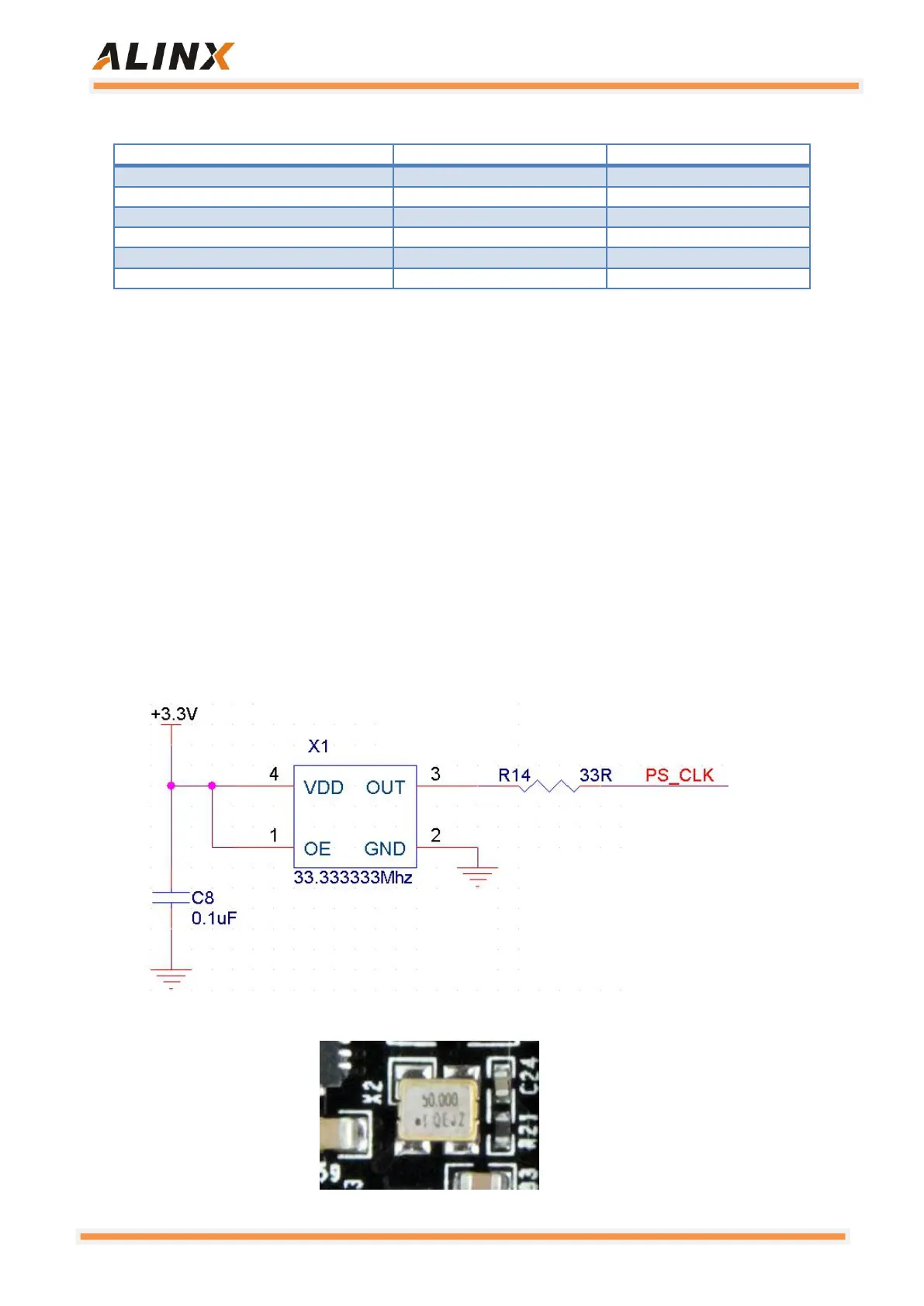
PS system clock source
The ZYNQ chip provides a 33.333 MHz clock input to the PS section
through the X1 crystal on the development board. The input of the clock is
connected to the pins of PS_CLK_500 of the BANK500 of the ZYNQ chip. The
schematic diagram is shown in Figure 2-6-1:
Figure 2-6-1: Active crystal oscillator to the PS section
Figure 2-6-2: 33.333Mhz active Crystal Oscillator on the Core Board