ZYNQ FPGA Development Board AX7021 User Manual
l
Amazon Store: https://www.amazon.com/alinx
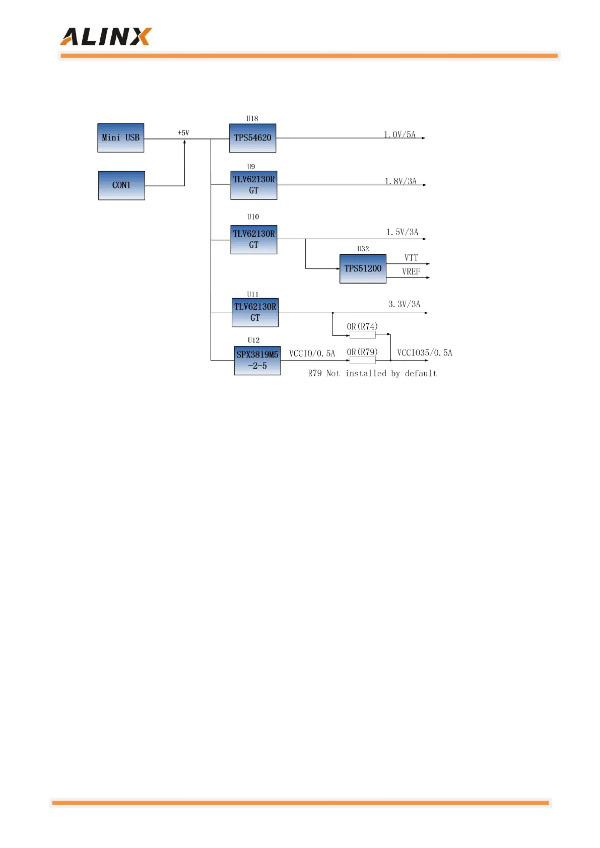
USB and the extension board at the same time to avoid damage. The power
supply design on the core board is shown in Figure 2-12-1.
Figure 2-12-1: The Power Supply Design on the Core Board
The development board is powered by +5V, and is converted into +1.0V,
+1.8V, +1.5V, +3.3V four-way power supply through four-way DC/DC power
supply core TPS54620TLV62130RGT. The output current of +1.0V can be as
high as 5A, and the other three output current are 3A. The VCCIO 2.5V power
supply is generated by one LDO SPX3819M5-2-5. The VCCIO 2.5V power
supply is mainly reserved for the BANK power supply of the BANK33 of the
FPGA. The user can select the power supply of BANK33 and BANK34 through
two 0 ohm resistors (R74, R79). By default, the R74 on the development board
is installed, and the resistor of R79 is not installed, so the power supply of
BANK33 and BANK34 is +3.3V. The user can replace the resistor so that the IO
of the BANK33, 34 outputs a voltage standard of 2.5V. 1.5V generates the VTT
and VREF voltages required by DDR3 through TI's TPS51200. The functions of
each power distribution are shown in the following Table 2-12-1: