ZYNQ FPGA Development Board AX7021 User Manual
l
Amazon Store: https://www.amazon.com/alinx
ZYNQ PS and PL section core voltage
ZYNQ PS and PL partial auxiliary voltage,
BANK501 IO voltage, eMMC
ZCNQ Bank0, Bank500, Bank13, Bank35,
VCCIO,QSIP FLASH, Clock Crystal
Reserved for ZYNQ Bank33,Bank 34
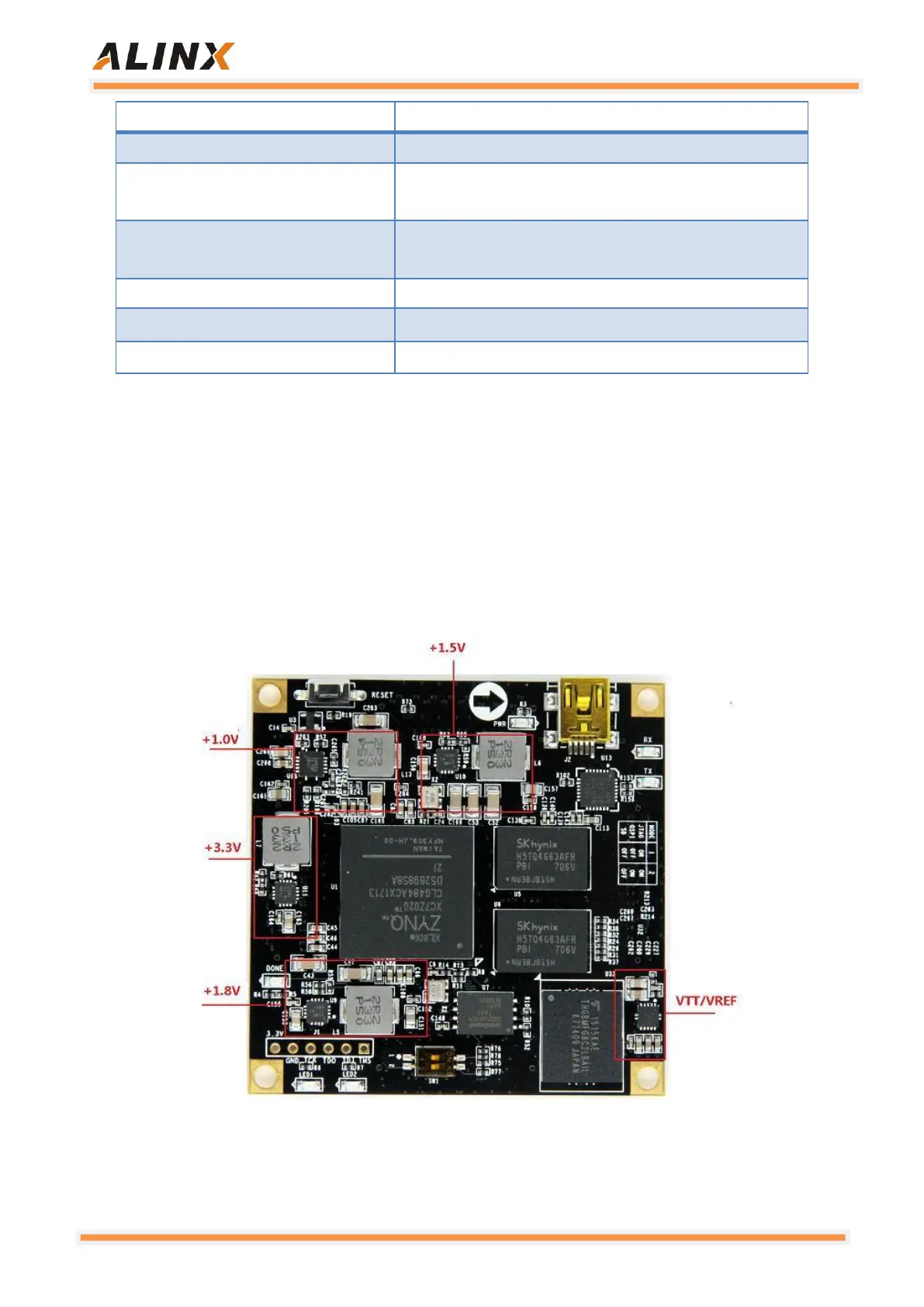
Table 2-12-1: The Functions of Each Power Distribution
Because the power supply of ZYNQ FPGA has the power-on sequence
requirement, in the circuit design, we have designed according to the power
requirements of the chip, and the power-on is +1.0V->+1.8V->(+1.5 V, +3.3V,
VCCIO). The circuit design ensures the normal operation of the chip. The
power supply on the core board detailed as Figure 2-12-2 below
Figure 2-12-2: The Power Supply on the Core Board