VCU118 Board User Guide 119
UG1224 (v1.5) March 15, 2023
AppendixC: BPI Flash Memory for VCU118 Boards Prior to Revision 2.0
Linear BPI Flash Memory
[Figure 2-1, callout 6]
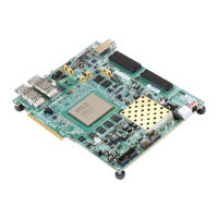
The linear BPI flash memory located at U133 provides 128 MB (1 Gbit) of nonvolatile
storage that can be used for configuration or software storage. The data, address, and
control signals are connected to the U1 XCVU9P bank 65. The BPI flash memory device is
packaged in a 64-pin BGA.
• Part number: MT28GU01GAAA1EGC-0SIT (Micron)
• Supply voltage: 1.8V
• Datapath width: 16 bits (with 26 address lines and 7 control signals)
• Data rate: up to 90 MHz
The linear BPI flash memory can synchronously configure the FPGA in master BPI mode at
the 90 MHz data rate supported by the MT28GU01GAAA1EGC flash memory by using a
configuration bitstream generated with BitGen options for synchronous configuration and
for a configuration clock division of one. The fastest configuration method uses the
external 90 MHz oscillator connected to the FPGA bank 65 EMCCLK pin AL20. By default,
UltraScale FPGAs use the parallel NOR flash asynchronous read in the master BPI
configuration mode.
A full XCVU9P 641,272,864-bit uncompressed bitstream requires 60% of the 1 Gbit linear
BPI NOR flash size, so one XCVU9P bitstream is supported.
The BPI flash memory upper address A25 pin is wired to pull-up header J29 to allow one of
two compressed bitstreams to be manually selected.
See the UltraScale Architecture Configuration User Guide (UG570) [Ref 2] for more
information.