VCU118 Board User Guide 67
UG1224 (v1.5) March 15, 2023
Chapter3: Board Component Descriptions
PCI Express Endpoint Connectivity
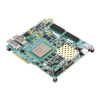
[Figure 2-1, callout 17]
The 16-lane PCI Express edge connector U2 performs data transfers at the rate of 2.5 GT/s
for Gen1 applications, 5.0 GT/s for Gen2 applications, and 8.0 GT/s for Gen3 applications.
The PCIe transmit and receive signal data paths have a characteristic impedance of
85Ω ±10%. The PCIe clock is routed as a 100Ω differential pair.
The XCVU9P-L2FLGA2104 (-2 speed grade) is deployed on the VCU118 to support up to
Gen3 x8 on VCU118 pre-Rev. 2.0 boards where V
CCINT
= 0.72V. PCI Express Gen3 x16
operation is not supported when V
CCINT
= 0.72V.
See the Virtex UltraScale+ FPGAs Data Sheet: DC and AC Switching Characteristics (DS923)
[Ref 1]. On VCU118 Rev. 2.0 and later boards, V
CCINT
= 0.85V and PCIe Gen 3 x16 is
supported.
When creating FPGA designs for the VCU118, the correct V
CCINT
must be chosen in the AMD
Vivado tool. Choose the appropriate entry for the V
CCINT
on your board:
V
CCINT
: 0.85V xcvu9p-flga2104-2L-e-es1
V
CCINT
: 0.72V xcvu9p-flga2104-2LV-e-es1
The V
CCINT
value on your board can be found using the VCU118 System Controller Tutorial
(XTP447) [Ref 14] or via the FPGA internal SYSMON function: after Vivado has discovered
the XCVU9P in the JTAG chain, the SYSMON module is displayed on the upper left pane.
Double-click on the SYSMON icon, which opens a parameter measurement pane. In the
upper left of this pane, click on the + option and a list of available parameters will be
displayed. Choose V
CCINT
, and the voltage value will be displayed.
The PCIe reference clock input is from the U2 edge connector. It is AC coupled to FPGA U1
through the MGTREFCLK0 pins of Quad 225. PCIE_CLK_Q0_P is connected to U1 pin AL9,
and the _N net is connected to pin AL8. The PCI Express clock connection is shown in
Figure 3-10.