VCU118 Board User Guide 7
UG1224 (v1.5) March 15, 2023
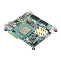
Chapter1: Introduction
Board Features
The VCU118 evaluation board features are listed here. Detailed information for each feature
is provided in Component Descriptions in Chapter 3.
• Virtex UltraScale+ XCVU9P-L2FLGA2104 device
•Zynq
™
7000 SoC XC7Z010 based system controller
• Two 2.5 GB DDR4 80-bit component memory interfaces (five [256 Mb x 16] devices
each)
• 288 MB 72-bit RLD3 memory interface comprised of two 1.125 Gb 36-bit devices
• Dual 1 Gb Quad SPI flash memory (BPI flash on pre-Rev. 2.0 boards)
• USB JTAG interface using a Digilent module with separate micro-B USB connector
• Clock sources:
°
Si5335A quad clock generator
°
Three Si570 I
2
C programmable LVDS clock generators
°
One SG5032 fixed 250 MHz LVDS clock generator
°
Si5328B clock multiplier and jitter attenuator for QSFP
°
Subminiature version A (SMA) connectors (differential)
• 52 GTY transceivers (13 Quads)
°
FMC+ HSPC connector (twenty-four GTY transceivers)
°
2x28 Gb/s QSFP+ connectors (eight GTY transceivers)
°
Samtec Firefly connector (four GTY transceiver)
°
PCIe 16-lane edge connector (sixteen GTY transceivers)
• PCI Express endpoint connectivity
°
Gen1 16-lane (x16)
°
Gen2 16-lane (x16)
°
Gen3 8-lane (x8) (Pre-Rev. 2.0 VCU118 board V
CCINT
= 0.72V)
°
Gen3 16-lane (x16) (VCU118 Rev. 2.0 and later V
CCINT
= 0.85V
• Ethernet PHY SGMII interface with RJ-45 connector
• Dual USB-to-UART bridge with micro-B USB connector
•I
2
C bus
• Status LEDs