VCU118 Board User Guide 46
UG1224 (v1.5) March 15, 2023
Chapter3: Board Component Descriptions
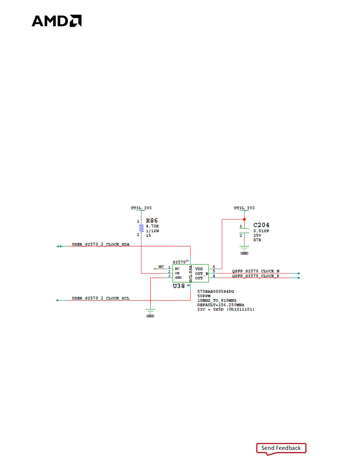
Programmable User Clock 2 (QSFP Clock)
[Figure 2-1, callout 13]
The VCU118 evaluation board has a SI570 I²C programmable low-jitter 3.3V LVDS
differential oscillator (U38) connected to FPGA U1 GTY bank 231 MGTREFCLK0 P/N pins W9
and W8 (series capacitor coupled), respectively.
On power-up, the U32 SI570 user clock defaults to an output frequency of 156.250 MHz.
The Zynq 7000 SoC system controller or FPGA user IP can change the output frequency
within the range of 10 MHz to 810 MHz through an I²C interface. Power cycling the VCU118
evaluation board resets the user clock to the default frequency of 156.250 MHz.
• Programmable oscillator: Silicon Labs Si570BAB0000544DG (10 MHz-810 MHz)
• Frequency tolerance: 50 ppm
• 3.3V LVDS differential output
The programmable clock circuit is shown in Figure 3-6.
X-Ref Target - Fig ure 3-6
Figure3‐6: VCU118 Board Programmable QSFP Clock