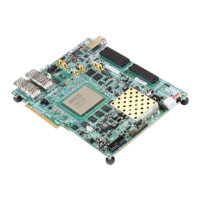
VCU118 Board User Guide 14
UG1224 (v1.5) March 15, 2023
Chapter2: Board Setup and Configuration
Default Switch and Jumper Settings
Switches
Default switch settings are listed in Table 2-2. Switch locations are shown in Figure 2-1.
Table 2-2 also references the respective schematic page numbers.
40
PCI Express Endpoint Connectivity, lane
width select header, (J7)
2x4 0.1 inch male header Sullins
PBC36DAAN
43
Notes:
1. VCU118 boards earlier than Rev. 2.0 host a linear BPI 16-bit flash configuration memory, 1 Gb (U133) Micron
MT28GU01GAAA1EGC-0SIT at location 6 and on their respective schematic page 54. See Appendix C, BPI Flash Memory for
VCU118 Boards Prior to Revision 2.0.
2. The VCU118 board schematics are available for download. See the VCU118 Evaluation Kit.
3. The VCU118 board jumper header locations are shown in Figure 2-2.
Table2‐1: VCU118 Board Component Descriptions (Cont’d)
Callout Feature Notes
Schematic
Page Number
Table2‐2: Default Switch Settings
Switch Function Default Comments
Figure 2‐1
Callout
Schematic
Page
SW1 SPST slide switch OFF Board shipped with power switch off 30 59
SW12 4-pole GPIO 0000 Positions 1-4, GPIO 26 55
SW15 4-pole configuration 0000
Positions 1-4, Zynq 7000 SoC System
Controller U111
28 49
SW16
4-pole configuration
(0 = Off/Open)
0001
Position 1, System Controller Enable
Positions 2-4, FPGA U1 mode
M[2:0] = Master SPI
35 3
Notes:
1. DIP switches are active-High (connected net is pulled High when DIP switch is closed).