VCU118 Board User Guide 82
UG1224 (v1.5) March 15, 2023
Chapter3: Board Component Descriptions
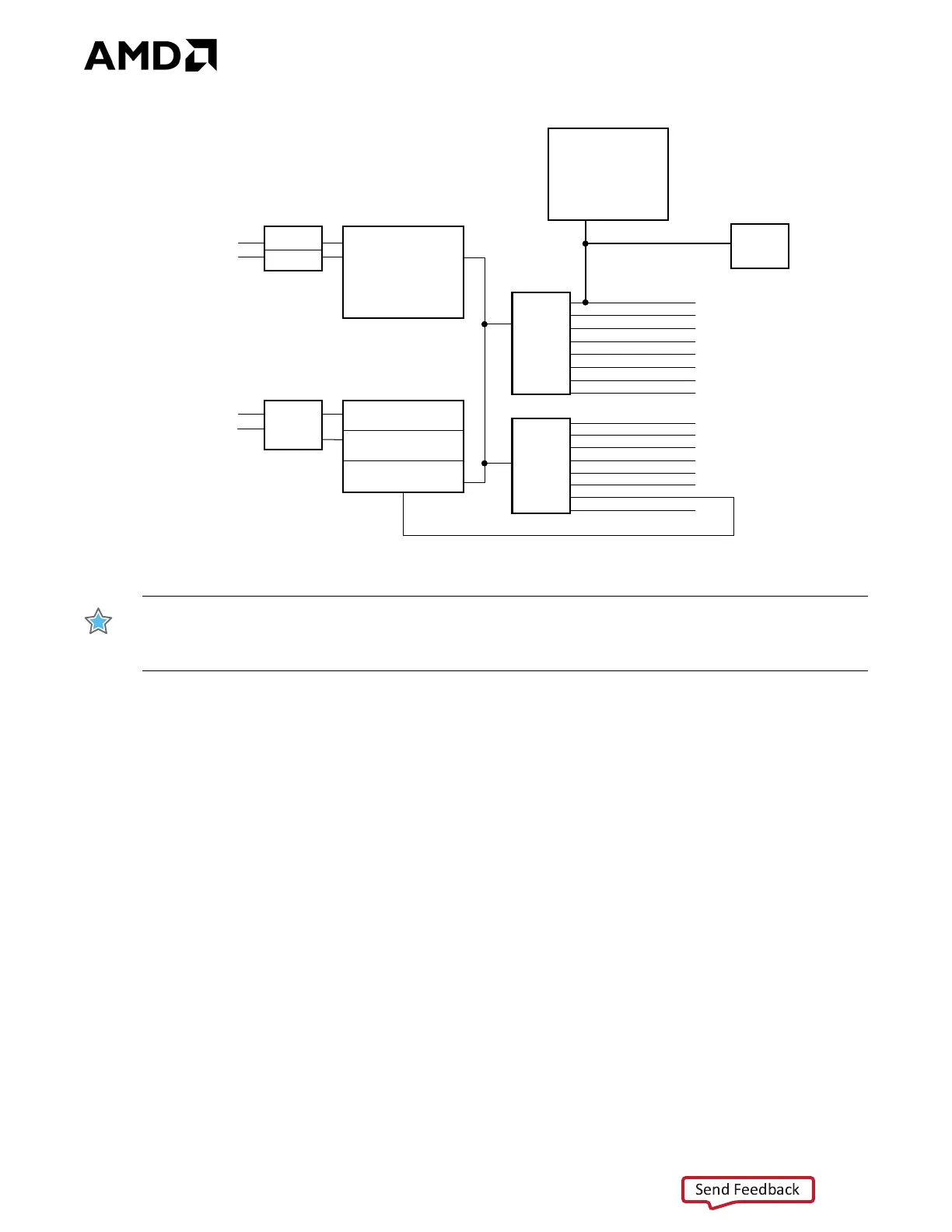
IMPORTANT: The TCA9548 U28 and U80 RESET_B pin 3 is connected to FPGA U1 Bank 64 pin AL25.
FPGA pin AL25 LVCMOS18 net IIC_MUX_RESET_B must be driven High to enable I²C bus transactions
with the devices connected to U28 and U80.
X-Ref Target - Figure 3-18
Figure3‐18: VCU118 IIC Bus
SYS Controller
U111
Level
shifters
always
enabled
SYS_1V8
BANK 501
Level
shifter
always
enabled
UTIL_3V3 to SYS_1V8
U109
MAXIM_CABLE_B
PMBUS_ALERT
MAXIM_CABLE_B
PMBUS_ALERT
UTIL_3V3 to VCC1V2_FPGA
Q27
IIC MUX
TCA9548
PMBUS
FMCP_HSPC
FMC_HPC1
EEPROM
0x75
0x11-0x1B, 0x70-0x73
0xx##
0xx##
0x54
IIC MUX
TCA9548
0x74
SI570 x1
NC
QSFPI
0x5D
0x50
SI570_0
SYSMON
0x68
0x5D
0x32
SI5328
Maxim power
regulators
12V_SW
Maxim
Cable
PMBUS SDA, SCL
0x10 – 0x18
U80
U28
Q23
Q21
UTIL_3V3 to
VCC1V8_FPGA
BANK 42
VCC1V2_FPGA
VCC1V8_FPGA
BANK 64
BANK 65
VCC1V8_FPGA
SYSMON IIC
FPGA U1
IIC_MAIN
INA_PMBUS
SI570_2
NC
0x40-0x45, 0x48
0x5D
NC
FIREFLY
QSFP2
0x50
0x50
X18025-041818