OMNIBUS II FEATURES
There are a number of formats for IRIG timing. The OmniBus II family uses the
IRIG formats indicated in Table 4.1. The characteristics of the external electrical
interface to the IRIG pins are as shown in Table 4.2 and Table 4.3.
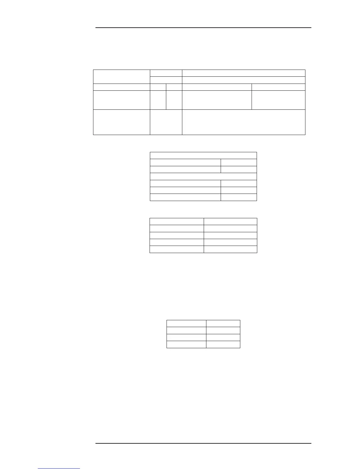
Format
Modulation Frequency
0 1 Pulse width coded Amplitude modulated
2
3
No carrier/index count interval
1 kHz/1 ms (B only)
10 kHz/.1 ms (A only)
Coded Expressions
0, 1, 2, 3, 4,
5, 6, 7
TOY
YEAR
System Timestamp only reflects BCD
TOY
CF can be set to or read from a register
SBS are ignored on input and 0 on output
Table 4.1—Input and Output IRIG formats
AM IRIG Input Characteristics
Min input impedance (at 1kHz)
Max input amplitude (V
pk-pk
)
AM IRIG Output Characteristics
Output mark amplitude (V
pk-pk
)
Output space amplitude (V
pk-pk
)
Max output resistive load
Table 4.2—Electrical characteristics of the AM IRIG signals
Output level
0 to 5 volts
Table 4.3—Electrical characteristics of the PCM IRIG signals
The following table lists the protocols supported on each pin. For information on
configuring and using the IRIG timer consult the BTIDriver API programming
manuals.
Note: The timing pins on the OmniBus II family are distinct and
not internally connected as they were in the OmniBus family.
PCM IRIG
Core A Pin 17
Table 4.4—IRIG pinout
4.4 Core Discretes
OmniBus products have both input and output discrete capability. OmniBus II
has eight bidirectional TTL level discretes per core which can be used as either
inputs or outputs. All OmniBus II core discrete inputs and outputs are TTL level.
Each discrete output line has a 5-volt TTL driver which can source or sink up to
8 mA and has an individual tristate control; the discrete input receiver is a 5-volt
tolerant device with high input impedance (10µA leakage current). When used as
OmniBus II PCIe/PXIe User’s Manual 4-3