OMNIBUS II FEATURES
4.5.1 Shunt Inputs
A shunt input circuit pin is pulled up to a voltage source through a resistor. A
load resistance applied between the pin and ground will shunt current from the
source and generate a voltage at the pin. The pin voltage is compared with a ref-
erence voltage for input state detection. There are two defined states: the “Open”
state in which a high impedance is applied to the pin, and the “Ground” state in
which a low impedance is applied to the pin.
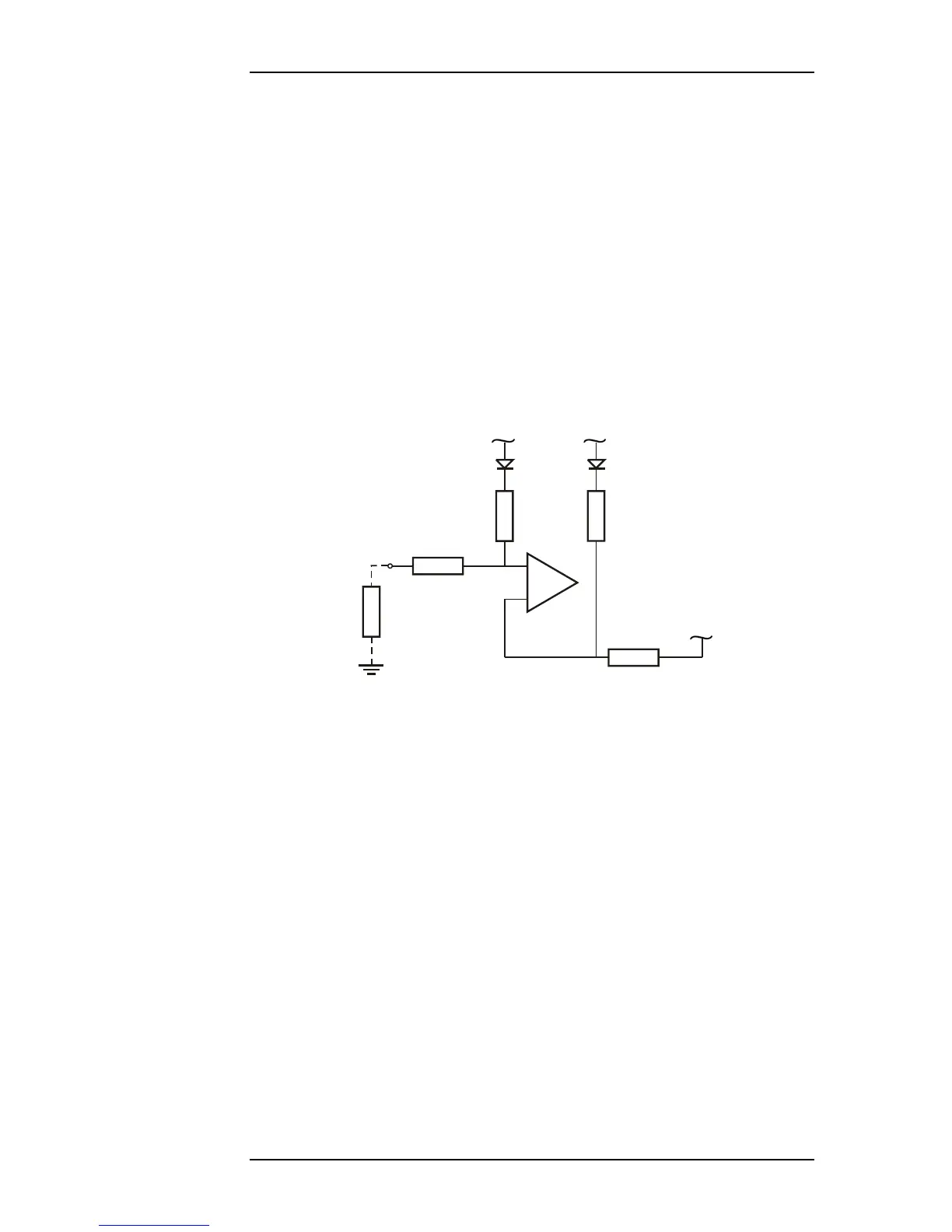
The OmniBus II discrete shunt input circuit, illustrated in Figure 4.2, has a 9 kΩ
pull-up resistor to a 5 volt source. An isolation diode provides protection against
over-voltage at the pin. A load resistance connected between the input pin and
ground will shunt current from the 5 volt source, through the forward biased di-
ode and the 9 kΩ resistor. A series resistor limits current as a voltage is generated
across the load which is compared to a reference voltage produced by an identi-
cal configuration. This results in a 3.25 volt switching voltage.
Figure 4.2—OmniBus II Discrete Shunt Input Circuit
4.5.2 Shunt Input Considerations
Limits: The OmniBus II discrete shunt inputs can withstand up to 35 VDC ap-
plied to the pin. The discrete inputs are capable of interfacing with industry
standard avionics discrete signals.
4.5.3 Shunt Outputs
A shunt output is typically an open-collector circuit and is normally high imped-
ance. When driven, the output sinks current to ground in a low impedance state.
Shunt outputs can be used to communicate with an input discrete and/or to ener-
gize a load.
The OmniBus II discrete shunt output circuit, illustrated in Figure 4.3, is a low
side switch capable of sinking up to 200 mA of current to ground through the
external load (Zext). A diode protection circuit permits safe switching of induc-
tive loads. Over-load detection limits the sink current and shuts the device down
in an over-temperature condition. Each output circuit is wired in parallel with an
input circuit (not shown) providing self-monitor capabilities.
5 kΩ
5 V
9 kΩ
R
app
5 kΩ
3.25V
5 V
9 kΩ
OmniBus II PCIe/PXIe User’s Manual 4-5