TABLE OF CONTENTS
LIST OF FIGURES
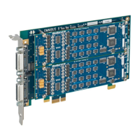
Figure 1.1—OmniBus II PCIe card ................................................................................ 1-1
Figure 1.2—OmniBus II PXIe card ................................................................................ 1-2
Figure 1.3—The two-core architecture of OmniBus II PCIe/PXIe card ......................... 1-3
Figure 2.1—PXIe Compatible Chassis Glyphs ............................................................... 2-2
Figure 3.1—Sample CoPilot screen ................................................................................ 3-1
Figure 4.1—Built-in test and System monitor architecture ............................................ 4-2
Figure 4.2—OmniBus II Discrete Shunt Input Circuit ................................................... 4-5
Figure 4.3—OmniBus II Discrete Shunt Output Circuit ................................................. 4-6
Figure 5.1—PXIe On-Board Clock Switch .................................................................... 5-1
Figure 5.2—PXIe Chassis Slot Glyphs ........................................................................... 5-5
Figure A.1—Transformer coupling to a dual-redundant databus .................................. A-2
Figure A.2—Direct connection to a dual-redundant databus ......................................... A-3
LIST OF TABLES
Table 4.1—Input and Output IRIG formats .................................................................... 4-3
Table 4.2—Electrical characteristics of the AM IRIG signals ........................................ 4-3
Table 4.3—Electrical characteristics of the PCM IRIG signals ...................................... 4-3
Table 4.4—IRIG pinout .................................................................................................. 4-3
Table 4.5—Hardware versus software designation of core discretes.............................. 4-4
Table 4.6—Avionics discrete I/O designations .............................................................. 4-7
Table 5.1—PXIe Trigger Signals.................................................................................... 5-2
Table 5.2—PXIe Trigger to Protocol Trigger Mapping ................................................. 5-3
Table 5.3—PXIe Trigger to Protocol Sync Mapping ..................................................... 5-3
Table 5.4—Transitional Protocol Trigger Parameters .................................................... 5-4
Table 5.5—PXIe Status Parameters ................................................................................ 5-4
Table 6.1—OmniBus II PCIe Host Part Numbering ....................................................... 6-1
Table 6.2—OmniBus II PXIe/cPCIe Host Part Numbering ............................................ 6-1
Table 6.3—MIL-STD-1553 Module Part Numbering .................................................... 6-2
Table 6.4—MIL-STD-1553 Level Function Definition.................................................. 6-2
Table 6.5—MIL-STD-1553 ParamAmplitudeConfig Configval .................................... 6-3
Table 6.6—MIL-STD-1553 ParamAmplitudeConfig Output Drive ............................... 6-3
Table 6.7—ARINC 429 Module New Applications Part Numbering ............................ 6-4
Table 6.8—ARINC 429 Module Deprecated Part Numbering ....................................... 6-4
Table 6.9—ARINC 429 Parametric Waveform Characteristics ..................................... 6-5
Table 6.10—MIL-STD-1553 Module Part Numbering .................................................. 6-6
Table 6.11—ARINC 708 ParamAmplitudeConfig Configval ........................................ 6-7
Table 6.12—ARINC 717 Module New Applications Part Numbering .......................... 6-7
Table 6.13—ARINC 717 Module Deprecated Part Numbering ..................................... 6-7
Table 7.1—General pin designations .............................................................................. 7-2
Table 7.2—Pinouts for MIL-STD-1553 modules ........................................................... 7-3
Table 7.3—Pinouts for ARINC 429 modules ................................................................. 7-4
Table 7.4—Pinouts for ARINC 708 modules ................................................................. 7-5
Table 7.5—Pinouts for ARINC 717 modules ................................................................. 7-6
Table 7.6—Wiring chart for 16036 cable assembly ....................................................... 7-8
Table 7.7—MIL-STD-1553 cable assembly configurations ........................................... 7-9
Table 7.8—Twinax wiring on MIL-STD-1553 cable assemblies ................................... 7-9
Table 7.9—D-sub connector pinout for cable assemblies 16037 and 16039 ................ 7-10
OmniBus II PCIe/PXIe User’s Manual iii