137
8025I–AVR–02/09
ATmega48P/88P/168P/328P
When the ICR1 is used as TOP value (see description of the WGM13:0 bits located in the
TCCR1A and the TCCR1B Register), the ICP1 is disconnected and consequently the Input Cap-
ture function is disabled.
• Bit 5 – Reserved Bit
This bit is reserved for future use. For ensuring compatibility with future devices, this bit must be
written to zero when TCCR1B is written.
• Bit 4:3 – WGM13:2: Waveform Generation Mode
See TCCR1A Register description.
• Bit 2:0 – CS12:0: Clock Select
The three Clock Select bits select the clock source to be used by the Timer/Counter, see Figure
13-10 and Figure 13-11.
If external pin modes are used for the Timer/Counter1, transitions on the T1 pin will clock the
counter even if the pin is configured as an output. This feature allows software control of the
counting.
13.11.3 TCCR1C – Timer/Counter1 Control Register C
• Bit 7 – FOC1A: Force Output Compare for Channel A
• Bit 6 – FOC1B: Force Output Compare for Channel B
The FOC1A/FOC1B bits are only active when the WGM13:0 bits specifies a non-PWM mode.
When writing a logical one to the FOC1A/FOC1B bit, an immediate compare match is forced on
the Waveform Generation unit. The OC1A/OC1B output is changed according to its COM1x1:0
bits setting. Note that the FOC1A/FOC1B bits are implemented as strobes. Therefore it is the
value present in the COM1x1:0 bits that determine the effect of the forced compare.
A FOC1A/FOC1B strobe will not generate any interrupt nor will it clear the timer in Clear Timer
on Compare match (CTC) mode using OCR1A as TOP. The FOC1A/FOC1B bits are always
read as zero.
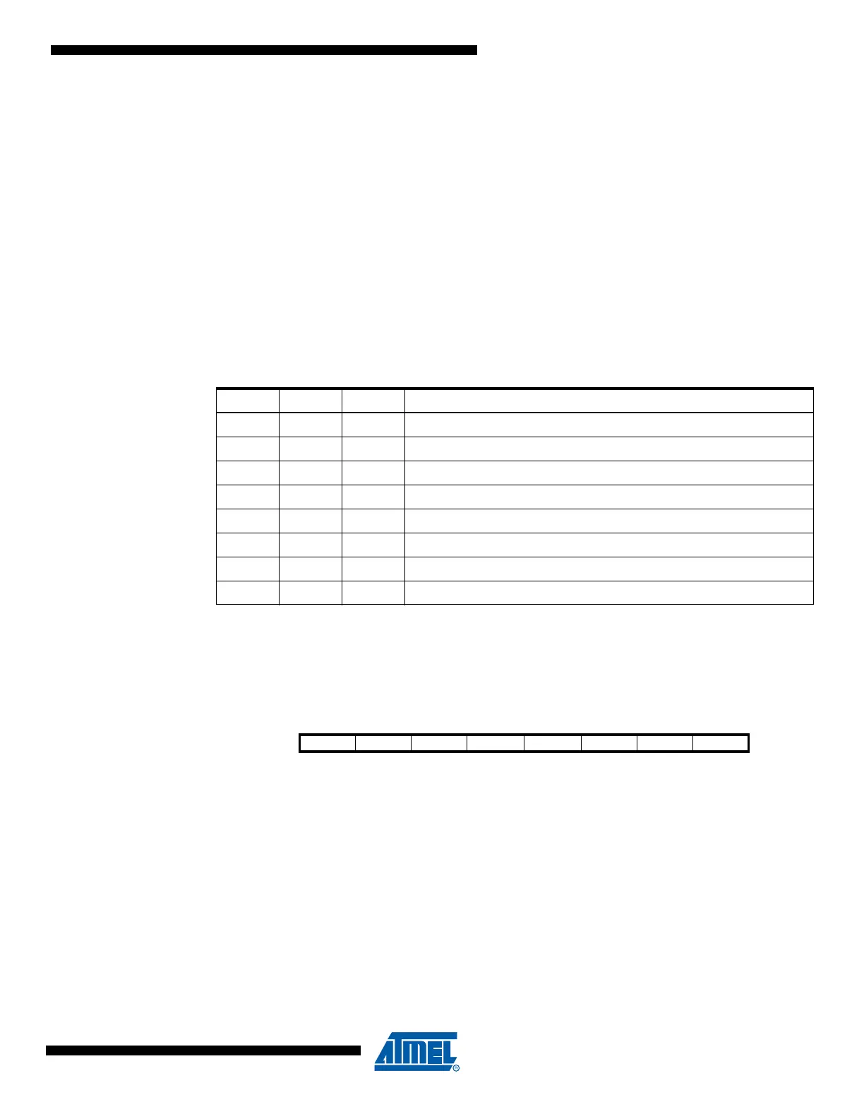
Table 13-5. Clock Select Bit Description
CS12 CS11 CS10 Description
0 0 0 No clock source (Timer/Counter stopped).
001clk
I/O
/1 (No prescaling)
010clk
I/O
/8 (From prescaler)
011clk
I/O
/64 (From prescaler)
100clk
I/O
/256 (From prescaler)
101clk
I/O
/1024 (From prescaler)
1 1 0 External clock source on T1 pin. Clock on falling edge.
1 1 1 External clock source on T1 pin. Clock on rising edge.
Bit 7 6 5 4 3 2 1 0
(0x82) FOC1A FOC1B – – – – – – TCCR1C
Read/Write R/W R/W R R R R R R
Initial Value 0 0 0 0 0 0 0 0