90
8025I–AVR–02/09
ATmega48P/88P/168P/328P
• INT0/PCINT18 – Port D, Bit 2
INT0, External Interrupt source 0: The PD2 pin can serve as an external interrupt source.
PCINT18: Pin Change Interrupt source 18. The PD2 pin can serve as an external interrupt
source.
• TXD/PCINT17 – Port D, Bit 1
TXD, Transmit Data (Data output pin for the USART). When the USART Transmitter is enabled,
this pin is configured as an output regardless of the value of DDD1.
PCINT17: Pin Change Interrupt source 17. The PD1 pin can serve as an external interrupt
source.
• RXD/PCINT16 – Port D, Bit 0
RXD, Receive Data (Data input pin for the USART). When the USART Receiver is enabled this
pin is configured as an input regardless of the value of DDD0. When the USART forces this pin
to be an input, the pull-up can still be controlled by the PORTD0 bit.
PCINT16: Pin Change Interrupt source 16. The PD0 pin can serve as an external interrupt
source.
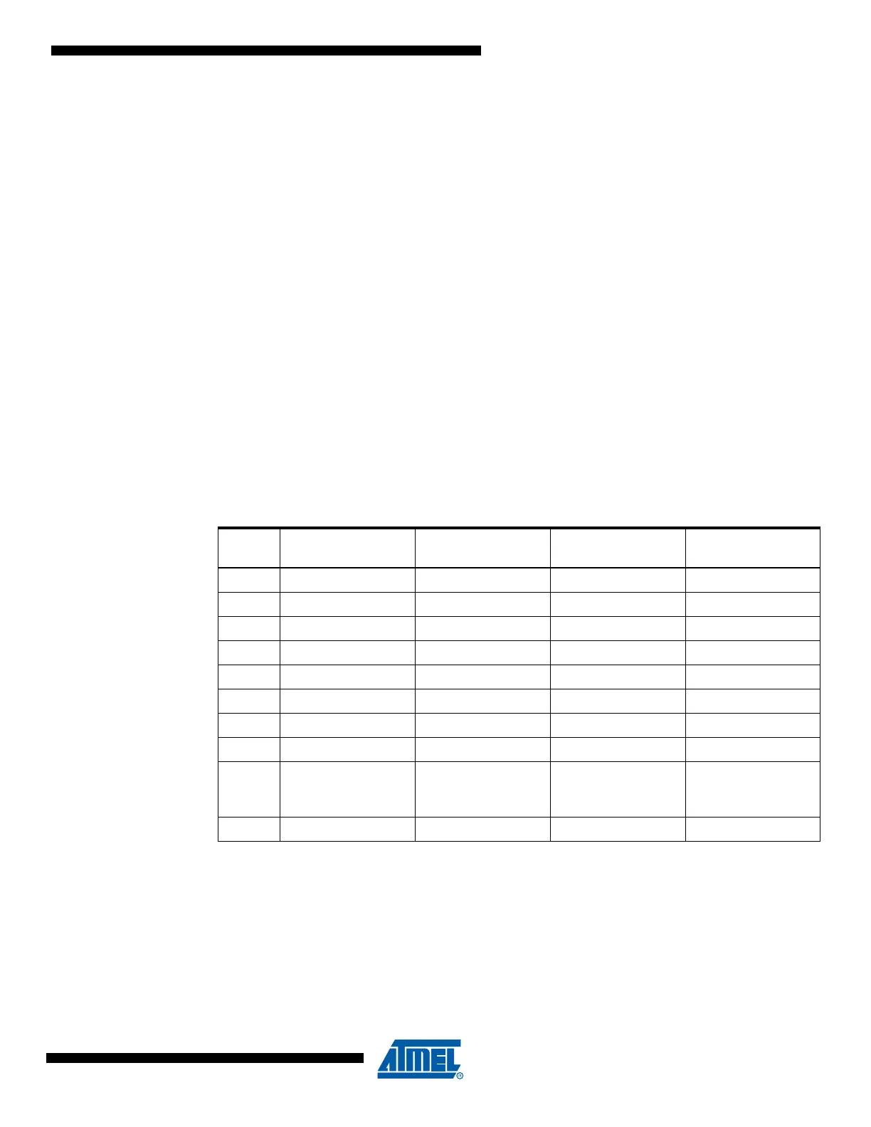
Table 11-10 and Table 11-11 relate the alternate functions of Port D to the overriding signals
shown in Figure 11-5 on page 80.
Table 11-10. Overriding Signals for Alternate Functions PD7..PD4
Signal
Name
PD7/AIN1
/PCINT23
PD6/AIN0/
OC0A/PCINT22
PD5/T1/OC0B/
PCINT21
PD4/XCK/
T0/PCINT20
PUOE0000
PUO0000
DDOE 0 0 0 0
DDOV 0 0 0 0
PVOE 0 OC0A ENABLE OC0B ENABLE UMSEL
PVOV 0 OC0A OC0B XCK OUTPUT
DIEOE PCINT23 • PCIE2 PCINT22 • PCIE2 PCINT21 • PCIE2 PCINT20 • PCIE2
DIEOV1111
DI PCINT23 INPUT PCINT22 INPUT
PCINT21 INPUT
T1 INPUT
PCINT20 INPUT
XCK INPUT
T0 INPUT
AIO AIN1 INPUT AIN0 INPUT – –