50
7598H–AVR–07/09
ATtiny25/45/85
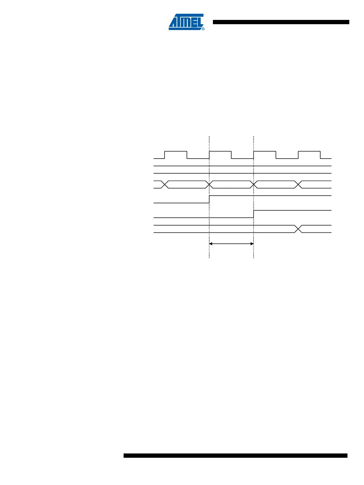
Consider the clock period starting shortly after the first falling edge of the system clock. The latch
is closed when the clock is low, and goes transparent when the clock is high, as indicated by the
shaded region of the “SYNC LATCH” signal. The signal value is latched when the system clock
goes low. It is clocked into the PINxn Register at the succeeding positive clock edge. As indi-
cated by the two arrows tpd,max and tpd,min, a single signal transition on the pin will be delayed
between ½ and 1½ system clock period depending upon the time of assertion.
When reading back a software assigned pin value, a nop instruction must be inserted as indi-
cated in Figure 10-4. The out instruction sets the “SYNC LATCH” signal at the positive edge of
the clock. In this case, the delay tpd through the synchronizer is one system clock period.
Figure 10-4. Synchronization when Reading a Software Assigned Pin Value
The following code example shows how to set port B pins 0 and 1 high, 2 and 3 low, and define
the port pins from 4 to 5 as input with a pull-up assigned to port pin 4. The resulting pin values
are read back again, but as previously discussed, a nop instruction is included to be able to read
back the value recently assigned to some of the pins.
out PORTx, r16 nop in r17, PINx
0xFF
0x00 0xFF
SYSTEM CLK
r16
INSTRUCTIONS
SYNC LATCH
PINxn
r17
t
pd