159
7679H–CAN–08/08
AT90CAN32/64/128
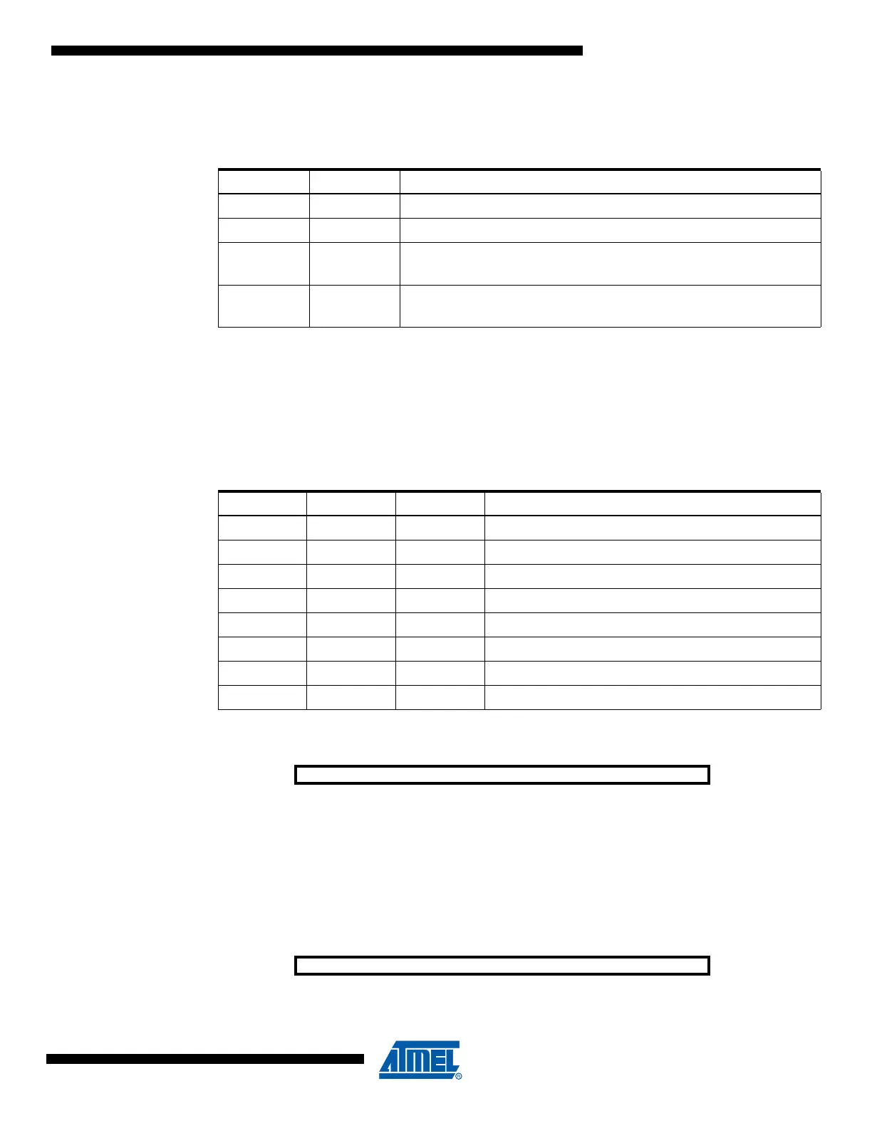
Table 14-4 shows the COM21:0 bit functionality when the WGM21:0 bits are set to phase cor-
rect PWM mode.
Note: 1. A special case occurs when OCR2A equals TOP and COM2A1 is set. In this case, the com-
pare match is ignored, but the set or clear is done at TOP. See “Phase Correct PWM Mode” on
page 153 for more details.
• Bit 2:0 – CS22:0: Clock Select
The three Clock Select bits select the clock source to be used by the Timer/Counter, see Table
14-5.
14.9.2 Timer/Counter2 Register – TCNT2
The Timer/Counter Register gives direct access, both for read and write operations, to the
Timer/Counter unit 8-bit counter. Writing to the TCNT2 Register blocks (removes) the compare
match on the following timer clock. Modifying the counter (TCNT2) while the counter is running,
introduces a risk of missing a compare match between TCNT2 and the OCR2A Register.
14.9.3 Output Compare Register A – OCR2A
Table 14-4. Compare Output Mode, Phase Correct PWM Mode
(1)
COM2A1 COM2A0 Description
0 0 Normal port operation, OC2A disconnected.
01Reserved
10
Clear OC2A on compare match when up-counting.
Set OC2A on compare match when downcounting.
11
Set OC2A on compare match when up-counting.
Clear OC2A on compare match when downcounting.
Table 14-5. Clock Select Bit Description
CS22 CS21 CS20 Description
0 0 0 No clock source (Timer/Counter stopped).
001clk
T2S
/(No prescaling)
010clk
T2S
/8 (From prescaler)
011clk
T2S
/32 (From prescaler)
100clk
T2S
/64 (From prescaler)
101clk
T2S
/128 (From prescaler)
110clk
T
2
S
/256 (From prescaler)
111clk
T
2
S
/1024 (From prescaler)
Bit 76543210
TCNT2[7:0] TCNT2
Read/Write R/W R/W R/W R/W R/W R/W R/W R/W
Initial Value00000000
Bit 76543210
OCR2A[7:0] OCR2A
Read/Write R/W R/W R/W R/W R/W R/W R/W R/W
Initial Value00000000

 Loading...


