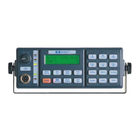
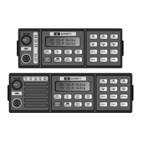
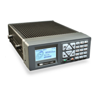
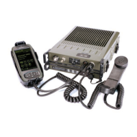
BARRETT 900 SERIES TRANSCEIVERS
Under normal operating conditions PA and Driver transistors will last indefinitely. The ALC circuit will fully
protect these transistors from incorrect antenna loads.
In data mode, if the cooling fan fails for any reason, a high temperature power reducing circuit will protect
these devices from overheating.
Damage to power transistors is rare and the reasons for failure should be properly investigated if a failed
transistor is found. Reasons for failure include lightning damage, power supply surges, and incorrect
adjustment of bias and power control circuits by users.
The driver transistors are either Philips type BLV11 or Motorola MRF433.
The PA transistors are Motorola type MRF455.
The procedure for replacement of driver and PA transistors is identical, so only the replacement of PA
transistors will be described in detail:
- Prior to removing the PA transistors, the base emitter and base collector junctions should be
checked for forward conduction and reverse leakage using a test meter. In order to do this, the
base leads must be desoldered using a large tipped iron preferably with a No. 8 (800 F) tip. The tab
is bent up to facilitate removal. The tab should be prized up clear of the PCB taking care not to
damage the transistor package. Forward and reverse junction resistance's can then be checked.
- Carefully remove all four M3 crosshead screws which hold the PA transistors in place. Store
them safely.
- Desolder the large 100R resistors and 10nF greencaps across the MRF455's.
- Desolder all the solder lugs connecting the flange to ground. Keep these safely. There should be
4 for a pair of transistors. Remove 2 spring washers from under the solder tags.
- Desolder the leads of the BD139 transistor which sits on top of the power transistor flange.
Remove this transistor for later use.
- Prize up the collector leads carefully until they are clear of the PCB. The collectors have a
bevelled tab.
- Prize up both opposed emitter tabs carefully. Extra heat is required here as they are connected to
the ground plane. Remove the transistors through the PCB access hole.
- Remove excess solder from the four PCB pads and clean them with isopropyl alcohol or
methylated spirits.
- Clean all traces of heatsink compound from chassis heatsink area under the transistor being
changed. Ensure that no dirt, swarf or other foreign matter is located where the transistors will sit.
- Clean the thermal contact surface of the replacement device. Smear a thin layer of heatsink
compound evenly onto the transistor seat. Push the transistor into place and "wriggle" it in-situ.
Remove the transistor and inspect the heatsink area to check that heatsink compound has
coated the seating area of the transistor. A thin but complete smear of compound should be
present. Do not apply too much or two little as poor thermal conductivity will result.
- Seat replacement PA transistors carefully in place having bent up collector and base tabs 3mm
from their ends. The bevelled collector tab should face the large PA transformer.
- Position BD139 transistor with metal face down on PA transistor flange.
5.7.8 Replacement of PA output and driver transistors
-
- Disconnect 12V power feed at rear of transceiver.
PAGE 38