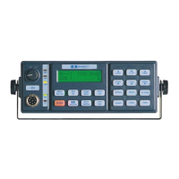
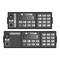
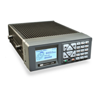
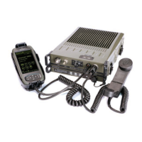
BARRETT 900 SERIES TRANSCEIVERS
The microprocessor has four sets of ports of its own used as follows:-
AN0 to AN7
CO1, CO0, CI, TO, INT2, SCK, RXD, TXD, PTTIN, CW KEY, ALESEN, GPSEN
PB0 to PB7
PA0 to PA7
Interrupts
4.1.6 DDFS and VCO
. These analogue input ports monitor transmit VSWR using voltages SWR+ and SWR-, receive
signal strength using voltage AGC, synthesiser lock state using voltage VCO Lock and battery voltage
utilising a voltage derived from a voltage divider consisting of R2 and R35. AN5 and AN6 are used to
measure voltages used to set up the selcall VCO tuning during the startup sequence. AN7 is used for
internal chassis temperature measurement, provided by sensor TS1, which is used for PA ALC trimming at
high temperatures.
CO1 and CO0 are counter/timer ports used to generate selcall transmit and alarm tones. CI and TO combine
to decode the received selcall pre -amble and data stream. INT2 is the main interrupt processing PTTIN and
CW KEY, SCK is unused. RXD and TXD are the external RS-232 serial ports. RXD and TXD are routed by
U44 and combinations of signals ALESEN and GPSEN to input and output data to and from an internally
fitted ALE controller option, as well as inputting data from either an external or internal GPS receiver. RESET
ALE is used to reset the ALE controller option when fitted.
is bi-directional and handles various slow speed input and output requirements such as Scan
Stop and Mute state.
handles further low speed signals including generation of annunciation beeps via signal
ALARM DATA.
are processed by the Interrupt Controller consisting of U18, U25 and U26. Lines PTTIN and CW
KEY are latched by signal ICP from the microprocessor. A magnitude comparator U25 compares the lines
with their previous state and requests an interrupt via INT2 if there is a state change.
The synthesiser employs a Direct Digital Frequency Synthesiser integrated circuit U7 which takes in
frequency data over the data bus with registers accessed by the 5 bit address field. The synthesiser is a dual
unit, half of which is used to generate 1/10 of the VCO frequency. The other half is the Carrier Insertion
Oscillator, the frequency of which is dependant on th type of I.F. filter used, and the mode of operation
chosen but is in the region of 455 kHz. The outputs of U7 are digitized sine waves which are decoded by
Digital to analog converters U8, U9, and U12. U8 and U9 are used to decode the VCO reference, and U12
decodes the carrier insertion output. T1 is a resonant transformer which yields a clean sine wave for the
carrier insertion signal.
In order to achieve a spurious free, low phase noise local oscillator, a high level(+13dBm) push pull VCO
operating at 10 times the DAC reference frequency is coupled to the DAC reference signal via a tracking
PLL.
Diodes D9, D10, D11, D12, D15, D16, D18, limit the voltage excursions on the FET gates maintaining
constant amplitude and low noise. An attenuator formed by resistors R187 to R189 and amplifier Q16 are
used to isolate the VCO from the low pass filter and first mixer circuits.
The VCO feeds the first mixer via a buffer amplifier comprising Q16 and T4 and a 76 MHz LPF consisting of
L10, L11, this provides some gain to present the mixer with a final LO1 level of 17 dBm and high reverse
isolation. It also feeds a cascode pre-scaler buffer consisting of Q8 and Q15 which has high reverse
isolation preventing unwanted sidebands on the VCO. U21 provides a further buffer for the divide by 10 pre-
scaler. This pre-scaler is a Johnson counter employing U23, U24 and U28. It is reset at power up by U29
which uses the same reset feed as the microprocessor. This ensures true counting.
The reference signal from the DACs at 1/10 VCO frequency is fed through an anti-alliasing filter L1, L2 and
through a common emitter buffer Q1 to the phase comparator.
A digital phase comparator using U21:B and U22 generates positive going differential error pulses at TP23,
TP24 according to the phase relationship of the DACs waveform and VCO/10. Charge balancing is
performed by the Charge Pump Q2, Q3, Q4 Q5 which integrates the error signal in a lead-lag loop filter C82,
C83, R58. This control or error signal can swing over the entire 0 to 10V range according to selected
frequency. It is fed to varactors D2, D6, D7 and D8 controlling the VCO frequency. The VCO frequency
range is 45 to 75 MHz being 45 MHz above the indicated frequency on the LCD display.
An out of lock red LED is driven by the phase comparator to provide fault indication. This signal also
generates a displayed error message and is used by the microprocessor to inhibit transmission if the VCO is
unlocked.
PAGE 15