3.2.9 Video circuit
1. Video circuit block diagram is shown as the following figure 3.2.9.1:
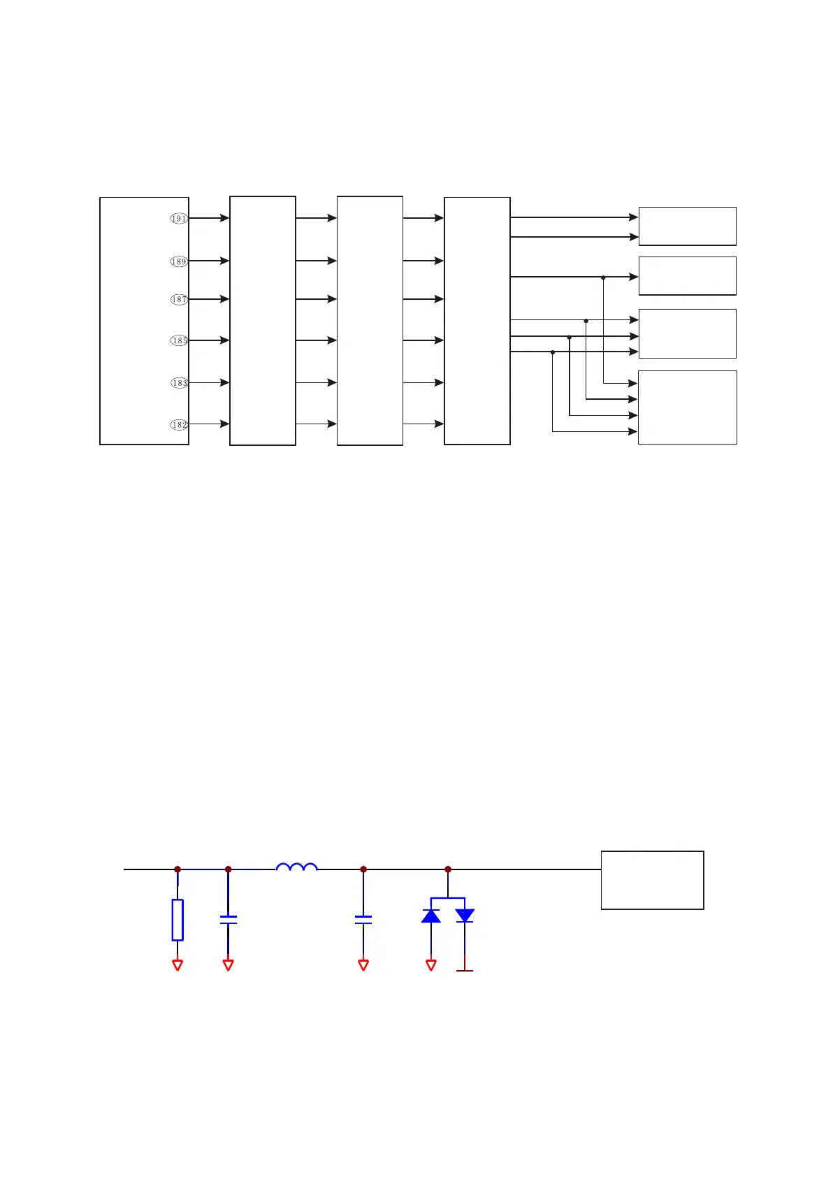
Figure 3.2.9.2 S-VIDEO output circuit diagram
R814
75R
C833
47P
C834
47P
L815 1.8uH
D+5V
VGNDVGND VGND VGND
Y1 VIDEO_Y
VD802
MMBD4148SE
S-VIDEO
2.Brightness signal, colour difference signal, CVBS signal and component video signal after being
decoded by MT1389 are sent out to the corresponding terminal for output after lowpass filtering and
clipping. Take Y1 signal as an instance, the following figure 3.2.9.2 shows the working principle of
filtering limiter circuit.
C833, C834 and inductor L815 compose a lowpass filter which
filters the high frequency interference signals beside useful ones; dual diode VD 802 is limiting circuit. It
is known from features of diode that the maximum amplitude of colour difference signal Y cannot exceed
5.7V and the minimum one cannot be under -0.7V, thus the high voltage signal from TV set can be
avoided burning down the player.
This circuit is very simple. R814 is a matched resistor, which makes the signal achieve the
maximum power on load. Capacitor
Component
video
Matching filter circuit
Catching circuit
Filter circuit
S-VIDEO
V-OUT
SCART
terminal
MT1389
Pr
Pb
Y1
V-OUT
C
Y
Figure 3.2.9.1 Video circuit block diagram
- 26 -