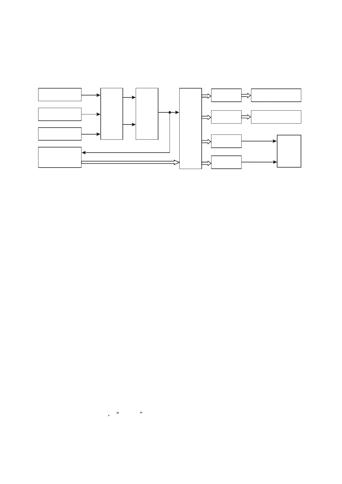
3.2.10 Audio power amplifying circuit block diagram
1. Audio power amplifying circuit block diagram is shown as the following figure 3.2.10.1:
Figure 3.2.10.1 Audio power amplifying circuit block diaghram
2. Working principle:
N505 (CD4052): CD4052 is a switch for selection, which is used to select externally inputted tuning
signal, MIC signal and left/right channel audio signal. When the player is in the state of playing disc, MIC
signal may be on. MIC changes to digital signal after conversion of CS5340, and this digital signal
outputs from pin 226 of MT1389 (SDATA0) to power amplifier board after outputting to decode for
processing.
N502 (CS5340): converse analog signal sent out from CD4052 to digital signal for processing by
back stage circuit.
N509 (TAS5508): after the processing of pulse width demodulation to SDA_AD, SDATA0, SDATA1,
SDATA2 digital audio signals, 8 channel outputs generate, that is, left/right channel output on
input/output board, front left/right channel on power amplifier board, surround left/right channel output,
subwoofer channel and centre channel output.
N507, N508 (TAS5112): is a high performance amplifying IC, which demodulates and amplifies
front left/right channel, surround left/right channel, centre and subwoofer after PWM of N509 (TAS5508).
3.2.11 HDMI circuit
1. Except for ordinary audio video output, this machine adds HDMI output. Block diagram of HDMI
is shown in figure 3.2.11.1 Source indicates facility with HDMI output jack and " Sink " indicates
facility with HDMI input.
External audio input
MIC signal input
TUNER
AUXR
AUXL
OK
TU_L
TU_R
N505
CD4052
AINR
N502
CS5340
AINL
SDA _AD
N509
TAS5508PAG
MT1389
OK
SDATA0,SDATA1,SDATA2
LO
RO
TAS51 12
N507
N508
TAS5112
N503
TLV272
N504
TLV272
Surround left/right channel
on power amplifier board,
subwoofer channel output
Front left/right channel on
power amplifier board,
centre channel output
AV board
left/right
channel
output
- 27 -