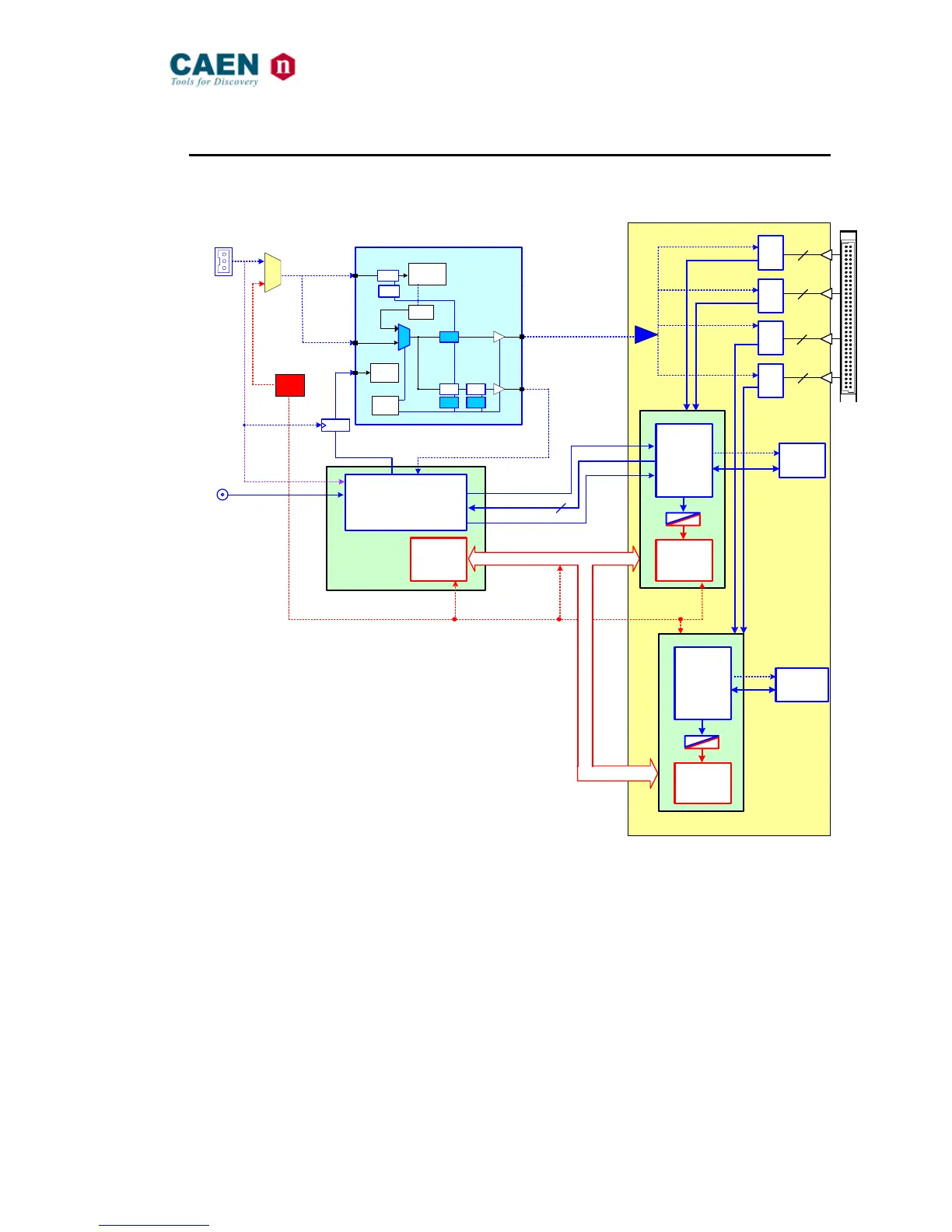
Fig. 3.2: Clock distribution diagram
The module clock distribution takes place on two domains: OSC-CLK and REF-CLK; the former is a
fixed 50MHz clock provided by an on board oscillator, the latter provides the ADC sampling clock.
OSC-CLK handles Local Bus (communication between motherboard and mezzanine boards; see
red traces in Fig. 3.2).
REF-CLK handles ADC sampling, trigger logic, acquisition logic (samples storage into RAM, buffer
freezing on trigger) through a clock chain. Such domain can use either an external (via front
panel signal) or an internal (via local oscillator) source, in the latter case OSC-CLK and REF-CLK
will be synchronous (the operation mode remains the same anyway).
DT5740 uses an integrated phase-locked-loop (PLL) and clock distribution device (AD9520). It is
used to generate the sampling clock for ADCs and mezzanine FPGA (SAMP-CLK0/SAMP-CLK1), as
well as the trigger logic synchronization clock (TRG-CLK).