3 Functional Description
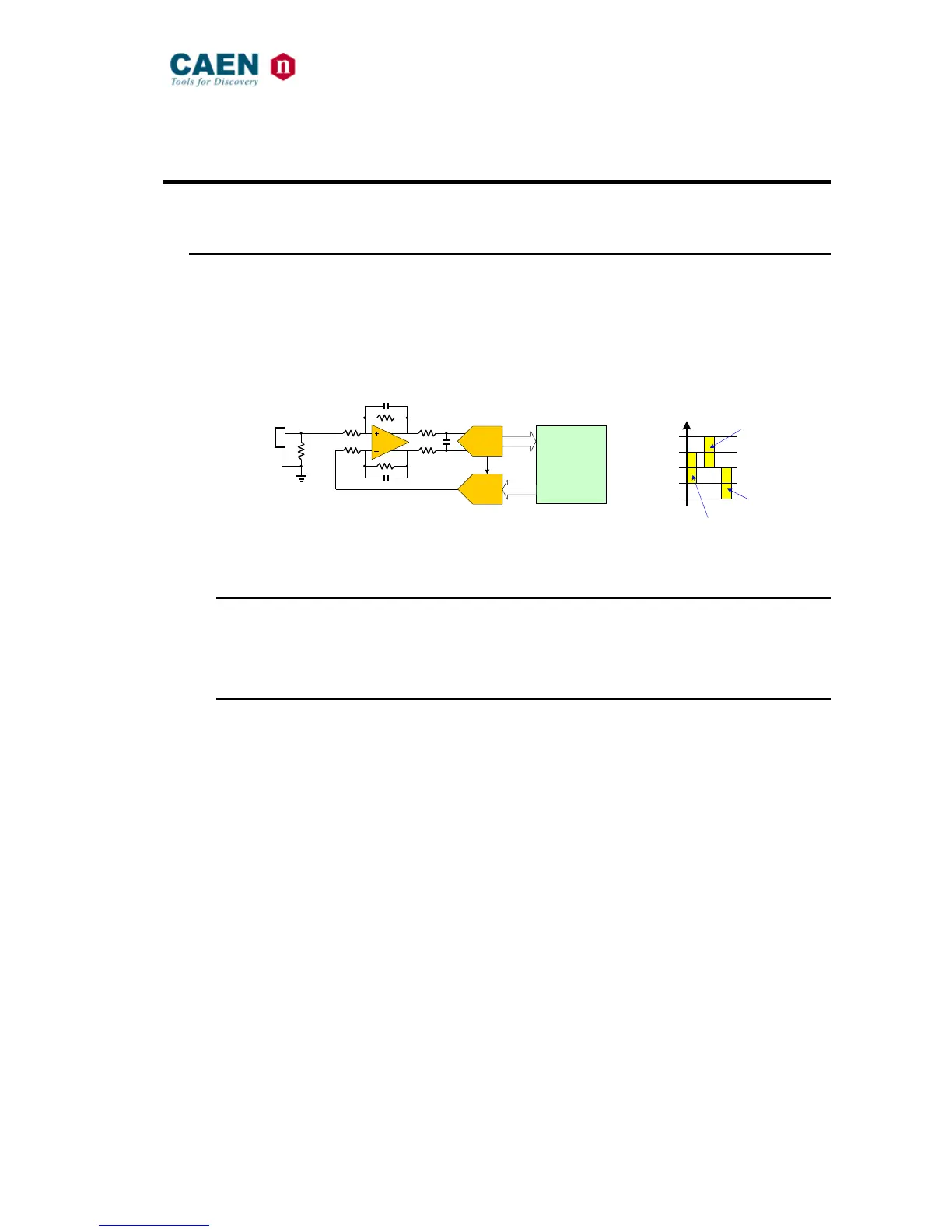
3.1 Analog Input
Input dynamic is 2V
pp
(Z
in
= 50 Ω). A 10V
pp
(Z
in
= 1 kΩ) dynamic is available on request. By means
of a 16-bit DAC it is possible to add up to a ±1V DC offset (±5V @10V
pp
) in order to preserve the
full dynamic range also with unipolar positive or negative input signals.
The input bandwidth ranges from DC to 30 MHz by 2nd order linear phase anti-aliasing low pass
filter.
Fig. 3.1: Input diagram
3.1.1 DC Offset Common Setting
Setting the DC offset requires a write access at register addresses 0x1n98. The DC offset value
will be then applied to all the 8 channels of group n.
3.1.2 DC Offset Individual Setting
It is possible to apply a 8-bit positive digital offset individually to each channel inside a group to
finely correct the baseline mismatch.
The two 32-bit registers that encode the eight unsigned values for group n (n = 0..7) are:
0x10C0 + 0x100 * n -> Correction values for channel offset 0..3
0x10C4 + 0x100 * n -> Correction values for channel offset 4..7
Please, see UM5483 - 740 Family Waveform Recording Firmware Registers document for details.
NOTE: DC Offset individual setting is supported from the mezzanine (AMC FPGA) firmware
revision 0.10 on.