5. CPU Board Resources
PC-686BX(NLX)-LV, PC-686BX(NLX)-LVV
33
5.
CPU Board Resources
I/O Map
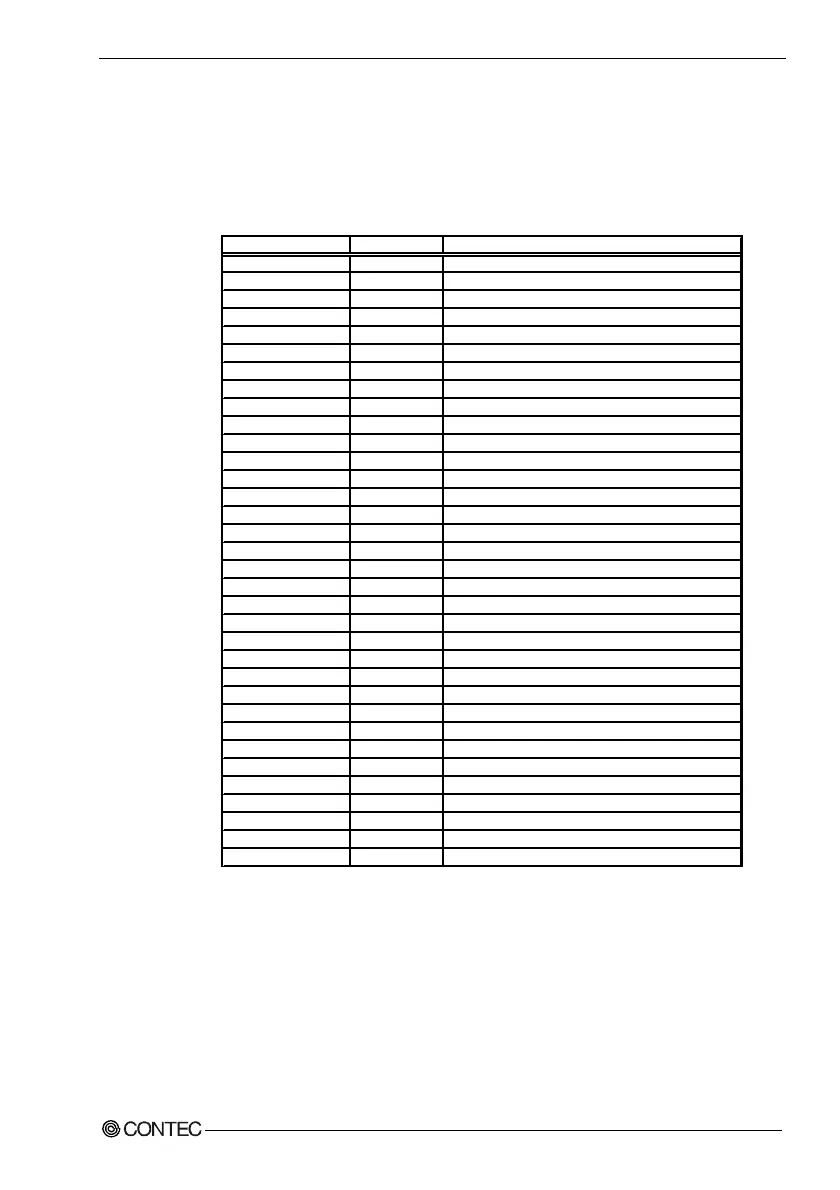
Table 5.1. I/O Port Address Map
Size
0000 ~ 000F 16 bytes DMA controller
0020 ~ 0021 2 bytes Interrupt control (PIC)
002E ~ 002F 2 bytes Super I/O controller configuration register
0040 ~ 0043 4 bytes System timer 1
0048 ~ 004B 4 bytes System timer 2
0060 1 byte Keyboard controller
0061 1 byte NMI, speaker control
0064 1 byte Keyboard controller
0070 ~ 0071 2 bytes Real time clock controller
0080 ~ 008F 16 bytes DMA page register
00A0 ~ 00A1 2 bytes Interrupt controller 2
00B2 ~ 00B3 2 bytes APM control
00C0 ~ 00DE 31 bytes DMA controller 2
00F0 ~ 00FF 16 bytes Math processor
0170 ~ 0177 8 bytes Secondary IDE controller
01F0 ~ 01F7 8 bytes Primary IDE controller
0228 ~ 022F* 8 bytes LPT3
0274 ~ 0277 4 bytes I/O read data port for ISA PnP attributes
0278 ~ 027F* 8 bytes LPT2
0295 ~ 0296 2 bytes Hardware monitor
02E8 ~ 02EF* 8 bytes COM4/Video (8514A)
02F8 ~ 02FF* 8 bytes COM2
0376 ~ 0377 2 bytes Secondary IDE channel
0378 ~ 037F 8 bytes LPT1
03B0 ~ 03BB 12 bytes Video (monochrome)
03C0 ~ 03DF 32 bytes Video (VGA)
03E8 ~ 03EF 8 bytes COM3
03F0 ~ 03F5, 03F7 8 bytes Diskette controller
03F6 1 byte Primary IDE channel
03F8 ~ 03FF 8 bytes COM1
04D0 ~ 04D1 2 bytes Edge or level-triggered PIC
LPT n + 400h 8 bytes ECP port, LPT n base address + 400h
0CF8 ~ 0CFF** 4 bytes PCI configuration address register
0CF9*** 1 byte Turbo/reset control register
Default (However, may be changed to different address range)
**