52
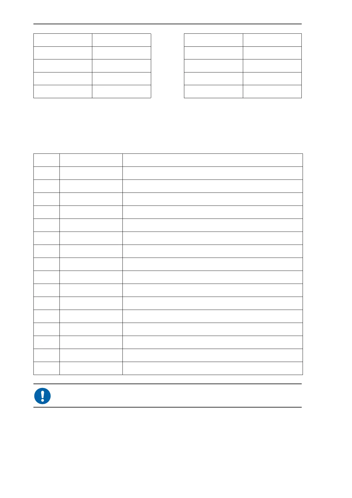
X4 – Test Interface, Load and Debug Connector
Connector is 2x8 pin male header, 2.54mm spacing
Table A.5: Pin order, connector X4
Note: this test interface is to be used only with adapter FAC1027.
c21 A(17) c5 D(12)
c20 A(18) c4 D(11)
c19 A(19) c3 D(10)
c18 A(20) c2 D(9)
c17 A(21) c1 D(8)
Pin Signal Description
1 D_CCLK Download, configuration clock, input
2 GND Signal ground for RS-232 ports A and B
3 D_FDIN Download, data in, input
4 RSATX Transmit data, RS-232 port A
5 D_BFGPADONE Download, Fpga configuration done, output
6 RSARX Receive data, RS-232 port A
7 D_CDIN Download, configuration data, input
8 RSBTX Transmit data, RS-232 port B
9 D_CDEN~ Download, configuration data enable, input
10 RSBRX Receive data, RS-232 port B
11 D_FPGAMODE Download, Fpga configuration mode select, input
12 VCC Supply output, +5V max 50mA
13 D_DOUT Download, data out, output
14 GND Signal ground for download signals
15 Not Connected
16 <No pin> Polarizing key