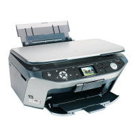
EPSON Stylus Photo RX585/RX595/RX610 Revision B
Operating Principles Operating Principles of Electric Circuitry 37
2.2 Operating Principles of Electric Circuitry
2.2.1 Overview
The major circuit boards of Stylus PHOTO RX585/595/610 are as follows:
Main Board: C693MAIN
Power Supply Board: C693PSB/PSE
Panel Board: C693PNL + C685PNL-B
2.2.2 Features
Based on the circuit mounted on the previous model Stylus PHOTO RX585/595/
610, this printer is equipped with an EEPROM and a reset circuit individually to
reduce the cost. This is achieved by removing a complex RTC circuit that is
mounted on the previous model.
With the increase in printing speed, the Case Open Sensor is newly added.
Equipped with a color LCD (2.5-inch TFD) as a standard feature
Power consumption reduced by executing the following actions at transition to the
power save mode
System control: Stopping part of clock inside the ASIC
Motor drivers entering sleep mode
Head DAC IC entering standby mode
Turning off power to the LCD
Printer control: Releasing the printer motor short brake
Cutting off the photo-electric current of the photo sensor
Scanner control: Stopping scanner motor chopping
Cutting off CIS & CIS LED current
Others: SDRAM entering self-refresh mode (automatic entering by ASIC
setting)
2.2.3 Circuit Board Constitution
Table 2-5. Circuit Board Constitution
Circuit Board Description
Main
Board
System
section
Oscillation circuit (48MHz ± 100 ppm)
SSCG setting circuit
ASIC incorporating CPU core (E01A73B*)
• Package: 352-pin PBGA
• Power voltage: Internal 1.0 V ± 0.1V External 3.3V ± 0.3V
•CPU core: V850E2
• Operation frequency: Inside of CPU core: 288MHz (SSCG)
SD-RAM controller: 96MHz (SSCG)
PT/ scanner section: 48MHz (SSCG)
Hardware JPEG decompression, AFP: 96MHz (SSCG)
Printer section: 48MHz (No SSCG)
Printer drive timer base clock: 48MHz (No SSCG)
• Built-in command RAM: 40 kByte (iLB-RAM)
• Built-in data RAM: 16 kByte (dLB-RAM)
Memory (FLASH ROM (64 Mbits), local SDRAM (256 Mbits), SERIAL
FLASH ROM (512 Kbits)
EEPROM (4Kbit)
Reset circuit
USB interface (both the HOST and DEVICE support High-Speed)
Panel interface
Color LCD interface
Power Supply
section
Power supply control circuit (PSC/ESAVE)
DC-DC converter circuit
Overvoltage protection circuit
Power-saving controller
Printer
section
Head drive circuit
CSIC interface
CR Motor control/driving circuit
PF Motor control/driving circuit
Sensor circuit
Card I/F
section
Memory card control ASIC (USX2007-NW-**)
Memory card connector (CF connector, 4 in 1 connector)
Power supply control circuit for CF
Scanner
section
Scanner motor control/driving circuit
Scanner interface circuit
Sensor circuits
Panel Board
LED lighting circuit
Switch reading circuit
Case open sensor circuit
Power Supply section
42 V generation circuit (flyback converter)
LCD Board
Module made by SEID (2.5-inch alpha TFD)
 Loading...