ES4455.2 Load Carrier Board - User’s Guide8
Introduction ETAS
1.1.2 Block Diagram
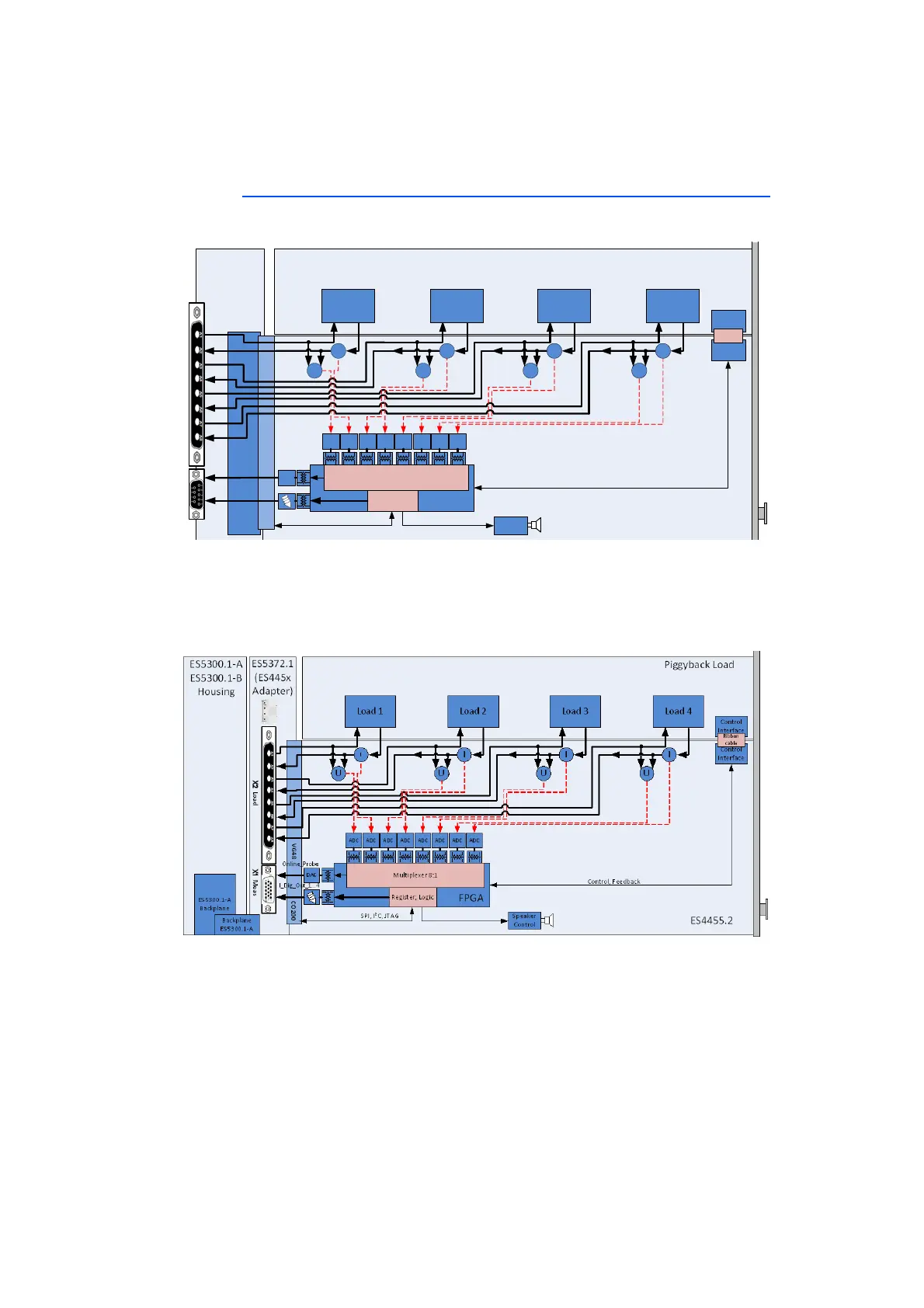
Fig. 1-1 shows a block diagram of the ES4455.2 Load Carrier Board with four
loads in the ES4408.1 Load Chassis.
Fig. 1-1 Block diagram of the ES4455.2 Load Carrier Board with loads,
installed in the ES4408.1 Load Chassis.
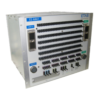
Fig. 1-2 shows a block diagram of the ES4455.2 Load Carrier Board with four
loads in the ES5300.1-A Housing or ES5300.1-B Housing.
Fig. 1-2 Block diagram of the ES4455.2 Load Carrier Board with loads,
installed in the ES5300.1-A Housing or the ES5300.1-B Housing.
Back-
plane
SPI, I²C, JTAG
ES4455.2_E
Control
Interface
Control
Interface
Ribbon
cable
ES4408.1
Load
Chassis
Control, Feedback
I
U
Load 1
I
U
Load 2
I
U
Load 3
I
U
Load 4
Speaker
Control
DAC
ADC ADC ADC ADC ADC ADC ADC ADC
Multiplexer 8:1
Register; Logic
FPGA
I_Dig_Out_1
...4
Online_Probe
Piggyback Load
Load 7, Load 8-1, Load 8-2
Meas 7, - 8-1, - 8-2
VG48 CO200