8842A
Instruction Manual
5-16
f5-09.wmf
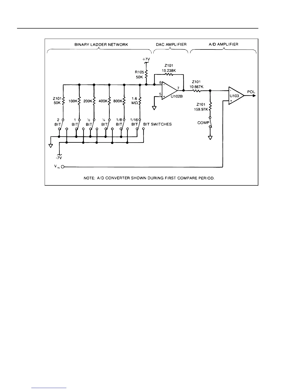
Figure 5-9. Analog-to-Digital Converter
The conversion process is broken up into an autozero period followed by five
measurement intervals. (A timing diagram is shown in Figure 5-5.) Six bits of the final
A/D sample are obtained during each interval.
During the first compare period (shown in Figure 5-9), the A/D Converter determines the
value of the scaled input voltage (Vin) by comparing Vin to the output of the DAC. Each
of the DAC bit-switches is tried in sequence and kept or rejected (left closed or reopened)
depending on the output polarity of the A/D Amplifier, which is configured as a
comparator. This process produces a string of six bits which is stored in the Timing/Data
Control circuit (the digital portion of U101).
During the following remainder-store period (Figure 5-10), the difference between the
Vin and the DAC output is multiplied by 16 by the A/D Amplifier and stored on
capacitor C102. During subsequent compare and remainder-store periods, the remainder
voltage is connected to the input of U103 and is resolved to six bits; the remainder
voltage (multiplied by 16) is stored alternately on capacitor C102 and C103. Each of the
five compare periods thus produces a six-bit nibble which is stored in the Timing/Data
Control circuit.