3-14
CIRCUIT
DESCRIPTIONS
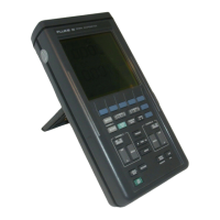
3,4 ANALOG CIRCUITS
(A2)
3.4.1 Introduction
This paragraph describes the
circuits or> the analog
A2
PCB
in detail. Refer to drcuit diagrams A2a.
A2b, and A2c (figures
10.5, 10.6, and 10.7 in chapter
10).
3.4.2
Overview analog circuits
The
analog A2 PCB contains several
functional parts:
•
circuits
In the acquisition
pati
-
attenuator
sections
•
EXTernal
(banana) Input/output circuitry
•
Analog
ASIC and AOC circuitry
•
control circuitry
-
signal generator
• power
supply and battery charger
Each of these
parts will be described
separately. First a short Introduction
is given, followed by
a
detailed description.
3.4.3 ATTENUATOR
sections, CHANNEL A and
B
-
Introduction
See figure 3.7.
The
attenuator sections of
both channels A and B are identical.
In the following only char^nel
A is
described. The corresponcSng
compor>ents for channel B have the
same numboiing, except the
second number, vrfiichis
’T
instead
of
'
2
'.
For example: R2202
in channel A corresponds with
R2102
fn channel B.
The attenuator section
consists of a ntgh frequency (here
after referred to as H.F.)
path and a low
frequency (here after
referred to as LF.) path, which
are combined again in the impedance
converter
(see figure 3.7). To
get a
flat
frequency charactehstlc, both
paths must overlap over
a
wide
frequency
range.
Circuits are provided for
automatic offset compensation.
The
output of the attenuator sections
of channel A and B is processed
further by the A-ASIC.