3-20
CtRCUIT DESCRIPTIONS
Protection
circuit (generator mode}
if a high voltage
is applied
to
the banana terminals
A and B, a
current will flow from terminal
A,
through PTC
(Positive Temperature Coefficient)
R2750,
zenerdiodes V2750 or
V2751
and v<a
V2752
and V2753 back to terminal B (see circuit
diagram
A2b,
figure
10.5).
The voltage across
the zener
diodes is limited to 7.5V for each diode. The rest of the input voltage is dropped across R2750. The
resistance of this PTC will rise and
limft
the
current
in
the
ctrcuit Opamp N2750
drives V2752
and
V2753, to prevent capacitive load of the generator by these zener diodes.
Protection (Ohm and diode
measurement)
If a
high voltage
is put on the EXT banana
terminals, this results In an irn^rease of the voltage over
PTC R2750.
This Increases the value of this PTC, limiting the current In the circuit. Zener diode
V2764 limits the output voltage
of
the measurtng amplifier arcuit N2751 . Resistor
R2771
and clamp
diodes V2759...V2763 protect the input of the measuring amplifier.
3.4.5 ANALOG ASIC (A-ASIC) and ADC circuitry
-
Introduction
See
figure 3.12.
The signals coming from the channel A and B attenuators are fed to D2301 . Various oscilloscope
functions are Integrated in this Application Specific Integrated Circuit (ASIC).
Analog ASIC D2301 selects the signal source and prepares the signal for further processing by the
ADC circuitry. Also a trigger signal is derived from one of the channel A or 8 inputs or the external
trigger
input
(banana
connectors).
-
Detailed circuit
description
See figure 3.12 and circuit
diagram A2a/A2b (figure 10.5/10.6).
First
a
short description is given for the internal circuits of the A-ASIC. The schematc diagram of the
A-ASIC D2301 is shown in figure 3.12. The A-ASiC input/output signals are also described in the
following sections.
Channei A
Amptifierand Channei B Amptifier
The output signals of the
charmel
A
and B attenuator sections are amplified In the A>ASIC to obtain
the most
sensitive
ranges.
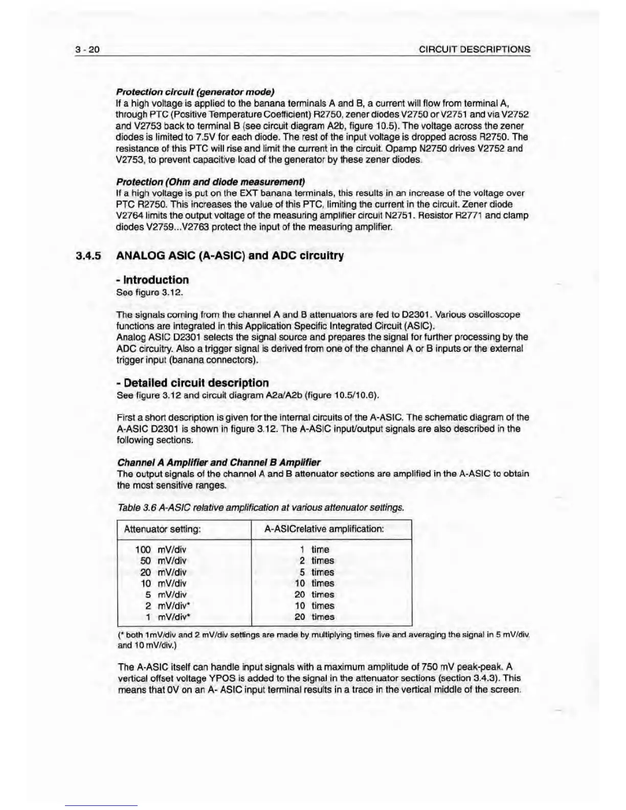
Table 3.6 A-ASIC relative amplification at varfous attenuator settings.
Attenuator setting: A-ASICrelatIve ampfificatlon:
100 mV/dlv 1 time
50
mV/div 2 times
20 mV/div 5
times
10 mV/di
V
10 times
5 mV/div 20
times
2
mV/div* 10 times
1
mV/diV 20 times
(*
both 1mV/dlv and 2 mV/div
settings are made by miitiptying times f<ve and averaging the signal in 5 mV/div.
ard 10 mV/div.)
The A-ASIC
itself can handle input signals with a maximum amplitude of 750 mV peak-peak. A
vertical offset voltage YPCS is added to the
signal
in
the attenuator sections (section 3.4.3). This
means that OV on an A-ASIC input
terminal results In
a
trace in the vertical middle of the screen.
 Loading...