GE HEALTHCARE
DIRECTION 5394141, REVISION 5 LOGIQ™ P5 SEVICE MANUAL
5-14 Section 5-4 - Main Board Detail
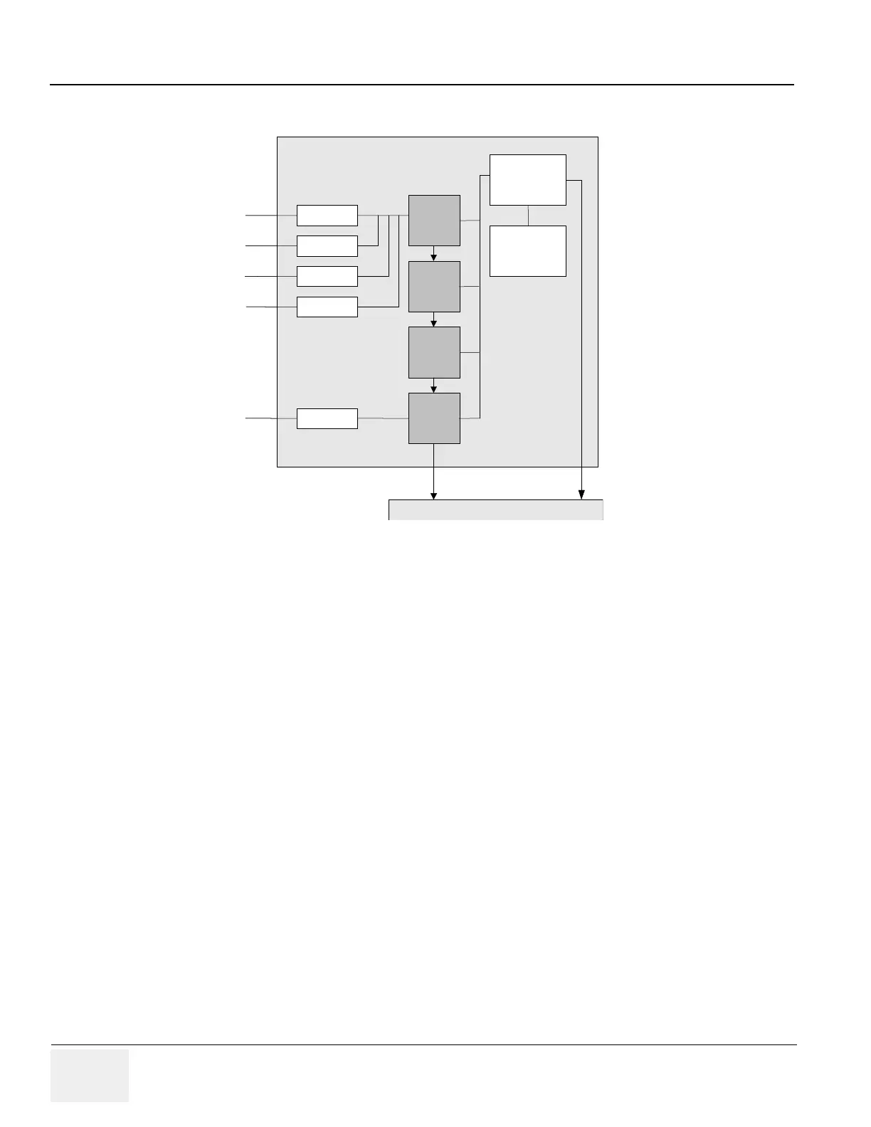
5-4-2-4 Delayed Sum Module
The Delayed Sum is the receive beam former and consist of 4 OQx2 ASICs. Each OQx2 ASIC has 16
receiving channels. The each digital beamforming output data of the OQx2 transferred to the next OQx2
and the output of final OQx2 transferred to the SYSCONPM(SYSCONCM)to make it into image data
through some digital signal processing.
Delay control data for receive beam forming are contained in SDRAM. Typically only 1 selected probe
data are saved in SDRAM. If new probe is connected, additional probe data will be downloaded from
HDD to SDRAM.
Main items are
• TRBC FPGA : Provide interfaces with SYSCONPM(SYSCONCM)through FE Bus. This FPGA
control all OQx2 asic for receive beamforming. All of parameter information for ASIC operation are
loaded into OQX2 ASIC from SYSCONPM(SYSCONCM) through this FPGA.
• OQX2 :Digital receive beamforming ASIC. Each OQX2 have capability of 16 channel receiving data
inputs. Each input data can be 12 bits. Operation clock is 40 MHz. 4 OQX2 ASICs are used in a
Delayed Sum module and each OQX2 summed output are cascaded to next OQX2 ASIC. So, the
last summed output of the last OQX2 are transferred to SYSCONPM(SYSCONCM) to make a
meaningful image data. The receive beamforming control logic in OQX2 ASIC need delay
information data for each channel's control logic. This delay information data are downloaded into
ASIC from SDRAM by TRBC FPGA.
• SDRAM(TD and RD Memory) : SDRAM keeps the receive delay data for OQX2 ASIC. During scan
time, these data are downloaded into OQX2 ASIC by TRBC FPGA. Memory capacity is 32Mbytes
for a probe.
Figure 5-13 DELAYED SUM Block Diagram
ADC 10bits
ADC 10bits
ADC 10bits
ADC 10bits
ADC 10bits
OQX2
OQX2
OQX2
OQX2
SDRAM
for
OQx2 & TPG2
Cl 1T RX
RF _ S UM
F
E
B
U
S
BACKPLANE ASSY
ADC 10bits
ADC 10bits
ADC 10bits
ADC 10bits
ADC 10bits
OQX2
OQX2
OQX2
OQX2
SDRAM
for
OQx2 & TPG2
Cl 1T RX
RF _ S UM
F
E
B
U
S
BACKPLANE ASSY